Stressing the eye: Testing receivers for jitter tolerance
Testing a receiver's ability to deal with impaired signals can determine how it will perform under real-world conditions.
By Guy Foster
SyntheSys Research
Stressed eye testing, otherwise known as receiver jitter tolerance testing, determines the ability of a high-speed electrical or optical receiver to deal with an impaired or imperfect incoming signal without misjudging ones for zeros, and vice versa.
Conceptually, most digital communication links--whether transoceanic fiber-optic links or high-speed connections across a circuit board or backplane--are similar. A clean signal is transmitted through a hostile environment and corrupted in various ways. The receiver's task is to reconstruct the original stream of ones and zeros without any errors.
At speeds above 1 Gbit/sec, a clock signal is encoded within most data signals as a timing reference that enables the receiver to correctly interpret the incoming data. Deriving the timing signal from the incoming data makes perfect sense, since the timing can be unexpectedly altered while passing between the transmitter and receiver.
A clock recovery circuit within the receiver attains a data-related clock signal from the data and uses it to time the execution of decisions on the incoming data, determining at each bit time slot whether the signal should be a one or zero. The decision circuitry instantaneously decides if the data in a bit time slot is above or below a predetermined threshold point for producing a clean one or zero.
This process works well, assuming the incoming data signals are perfect. But real-world signals carry "baggage" in the form of reduced amplitude, noise, or other impairments that produce jitter.
Controlling jitter
Jitter can best be explained as the non-ideal placement of data edges with respect to a clock. Data edges within the stream tend to move from their ideal positions and can begin interfering with the decision-making process of the receiver. As the edges begin moving across various bit cells, the likelihood of errors will increase.
The ability to recover an encoded clock from the data provides a major advantage. It enables the clock recovery circuit to produce a clock that can track the data signal as it moves around in time, acting as a jitter filter. The clock recovery circuit, however, is not effective against fast-moving signals or completely erratic movement. Clock recovery circuits switch over from tracking the jitter to fully passing the jitter at a frequency known as the loop bandwidth--usually a few MHz. But the ability to track slow-moving data signals still results in reduced jitter related to the recovered clock.
The application of sinusoidal jitter on a receiver with clock recovery can help determine the jitter tolerance of a specific device. This is accomplished by applying a jitter modulation of different frequencies and amplitudes to the incoming data signal, then recording errors as they occur. The test requires a bit-error ratio tester (BERT) and some type of impaired pattern source, often a sinusoidal modulation of the data signal transitions.
At low jitter frequencies, a receiver is often expected to endure large amounts of jitter, enough to close the test eye completely many times over. However, at low frequencies, the clock recovery should completely remove all jitter effects. At higher frequencies, less than one unit interval (UI) of jitter is applied.
The SONET/SDH world pioneered this method of measuring jitter tolerance. Each network link was designed with a transmit and receive end, with repeaters in between. Each repeater converted the optical signal back to the electrical domain, cleaned it, and amplified it enough to drive the conversion back to the optical domain and the distance to the next repeater. (This type of regeneration is less common following the invention of fiber amplifiers that reduced the need for conversions between optical and electrical domains along the way.) In such "repeatered" systems, signal-to-noise was the biggest impairment to system performance, but it was essential that repeaters didn't have the effect of amplifying jitter along the way, which is very possible in such systems.
Standardizing stressed testing
Jitter tolerance testing in repeatered SONET/SDH systems applied sinusoidal jitter to stress the clock recovery in the receivers because it was trackable. However, while that made sense in a repeatered SONET/SDH environment, many of the more recent standards have been tackling communication links of a very different sort. A commonality of today's systems, whether fiber-optic links or electrical cabling across backplanes and circuit boards, is that signal-to-noise often is not the limiting factor in performance.
Today's links are not just signal-to-noise limited in the amplitude axis; they can also suffer from inter-symbol interference (ISI) and crosstalk. As such, the signal must be subjected to both trackable (i.e. sinusoidal jitter) and untrackable (i.e. random jitter and bounded, uncorrelated jitter) stresses on the time axis.
Therefore, more complex methods of introducing impairments to a receiver under test are required to emulate these untrackable real-world stresses. Stressed eye testing is no longer simply a jitter test since it usually imposes restrictions around the entire eye, not just the time axis. A combination of several impairments, both trackable and untrackable, is needed to create an effective stressed signal.
The first standards to use stressed eye were Gigabit Ethernet and 1x, 2x, and 4x Fiber Channel, developed between 1998 and 2003. It was during this period that stressed eye was adopted and modified by the emerging 10-Gigabit Ethernet standard (2002). Since then, different recipes of stressed eye have been adopted in various standards, including high-speed buses, such as PCI Express and Serial ATA. A common theme in many standards is the amount of inferring and guesswork required to interpret the necessary information.
Signal impairments
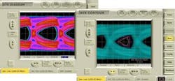
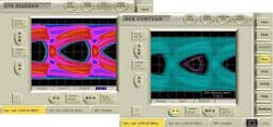
Each new stressed eye recipe intends to replicate whatever real-world impairments lay in wait for the receiver in its particular network. BER contours also provide a much deeper and detailed view of infrequent events, such as random jitter, that must be controlled to achieve true error-free operation. Figure 1 compares a typical eye diagram and a BER contour diagram for a serial ATA-compliant jitter tolerance test signal. The contours are like the contours on a geographic map, showing the steepness of mountains. In an eye, the steeper the slopes, the less likely the edges are going to intrude on the decision point and cause errors.
Several signal impairments are introduced to signals for testing the jitter tolerance of receivers under real-world conditions:
Putting it all together
Typically, a stressed eye test consists of two parts: Sinusoidal jitter, used to step through the different sinusoidal modulation frequencies and amplitudes, and a stressed recipe, sometimes in the form of an eye mask. The idea is to add various specified components to close the eye to an assured area of error-free operation in the center. The receiver is expected to operate successfully in this small area, despite the impairments.
Components can be set to a sinusoidal jitter template in several different ways, depending on the standard. Some standards, such as XFP, require the recipe to construct the eye to the mask without sinusoidal jitter. Once the mask is complied with, then the sinusoidal jitter template is stepped through. The other approach, used by standards such as 10-GbE and XAUI, constructs the stressed eye to the mask including sinusoidal jitter set to its highest frequency value (typically between 0.1 and 0.25 UI). The other components then are added to match the mask, and the sinusoidal jitter template is stepped through.
In either case, the goal is to introduce stressed eye stimulus to the receiver, step through the sinusoidal jitter template, and count the errors. Often, engineers will use the template as a basis but will step up the amplitude for a particular frequency until they reach the limit of performance to assess device margin (or move in the other direction to explore where a device failed compliance). Similarly, margin can be added in the eye template by making the error-free center smaller.
Whatever method is chosen, stressed-eye tests simulate real-world conditions to ensure that receivers will perform as advertised in the network. If receivers are exposed to the worst-case scenarios in the lab, they reasonably can be expected to meet or exceed any expectations of deployment.
Guy Foster is director of marketing at SyntheSys Research (Menlo Park, CA). He may be reached via the company's Web site at www.bertscope.com.
