Teramount and GlobalFoundries partnership focuses on new silicon photonic solutions

Teramount and GlobalFoundries are collaborating on ways to connect fibers to Silicon Photonics (SiPh) chips, addressing the growing bandwidth demands and power challenges in data and telecom applications.
As part of this collaboration, Teramount integrates its Universal Photonic Coupler solution with GF’s 45CLO silicon photonics platform, GF FotonixTM, to provide a scalable fiber packaging solution to customers who want to utilize high-speed optical connectivity for applications like AI/ML and data center.
This collaboration will enable deeper integration of optics into semiconductors through various packaging technologies that provide bandwidth, power, and latency performance scalability to the next generations of advanced computing applications.
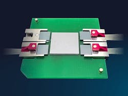
Teramount has been gaining momentum with its patented self-aligning optics technology. The company’s TeraVERSE product--a detachable and serviceable fiber connectivity product for assembly of Single-mode (SM) and Polarization-maintaining (PM) optical fibers on a silicon photonics chip—recently received a 5.0 rating on Lightwave’s 2024 Innovation Awards.
Comprised of Teramount’s detachable Photonic-Plug and a Photonic-Bump integrated into the customer’s silicon photonics chip using either Inverse Tapered Waveguides (wideband) or Grating Couplers (narrowband), TeraVERSE is optimized for Co-Packaged Optics (CPO) use case.
According to the company, its Photonic Plug and Bump components offer ±30µm / 0.5dB of assembly tolerances when aligning single-mode (SM) or polarization-maintaining (PM) fibers to a silicon photonics chip.
The Photonic-Plug uses wafer-level processes to place optical elements, shifting accuracy requirements from assembly to wafer manufacturing domain. Teramount’s Photonic-Bump aligns photonics with standard semiconductor manufacturing, packaging, and testing flows. The Photonic-Bump is a wafer-level optical element attached to the customer’s silicon photonics PIC wafer and accurately placed relative to a tapered waveguide using wafer-level processes.
Hesham Taha, Teramount’s President and CEO, said its customers “want to see it supported by leading foundries. GF’s feature-rich 45CLO Fotonix platform and position as a leading silicon photonics foundry make them an ideal partner for high-volume manufacturing of Teramount’s solution.”
For related articles, visit the Optical Tech Topic Center.
For more information on optical components and suppliers, visit the Lightwave Buyer’s Guide.
To stay abreast of optical communications technology, subscribe to Lightwave’s Enabling Technologies Newsletter.
About the Author

Sean Buckley
Sean is responsible for establishing and executing the editorial strategy of Lightwave across its website, email newsletters, events, and other information products.
Voices of the Industry