Integration - Manufacturing of planar lightwave circuits
Arrayed waveguide gratings, aided by advanced designs and precise manufacturing process control, potentially can replace hundreds of conventional piece parts.
DAVE RAUCH, Lightwave Microsystems Corp.
Next-generation optical networks require new functions and higher-performance optical components than exist in current legacy systems. For these systems to be practical, there must be significant reductions in the cost per optical function. A major challenge for component vendors is to provide increased functionality, at very high volumes, without increasing costs.
A leading approach to achieve this goal is through integration of multiple functions in a planar lightwave circuit (PLC). PLCs are optical circuits constructed of waveguides laid out on a silicon wafer and are constructed using tools and techniques advanced to extremely high levels by the semiconductor industry.
The high-volume manufacture of PLCs requires strict manufacturing systems, also derived from the semiconductor industry. The implementation of manufacturing control systems in a PLC wafer fab is essential to controlling fabrication processes and maintaining high yield and high performance.
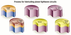
PLCs are optical circuits laid out on a silicon wafer (see Figure 1). A lower cladding layer of index nclad is deposited, followed by a core layer of index ncore, with ncore typically about 1% larger than nclad. The core layer is then patterned using standard photolithographic techniques, and a channel waveguide pattern is transferred to the core layer using various etching techniques.
In the example shown in Figure 1, a rib waveguide is produced by etching away the surrounding core using techniques such as reactive ion etching. It is possible to form a variety of other waveguides using different geometries and etching techniques. The channel waveguide is then covered by a top cladding layer, usually of the same index as the lower cladding, nclad. The end result is a buried channel optical waveguide on the substrate wafer.
Starting with such simple waveguide structures, very complex optical circuits can be fabricated. Arrayed waveguide gratings (AWGs) are already in widespread commercial use for multiplexing/demultiplexing in high-channel-count DWDM systems. AWGs represent a fairly high degree of integration. Commercial AWGs are available with 40 channels spaced at 50 or 100 GHz. Demonstrations of AWGs with 1281 channels and 2562 channels spaced at 25 GHz have been made in the laboratory, providing evidence that AWGs can scale to even higher channel counts. Furthermore, the insertion loss of an AWG does not increase linearly with channel count as it does for thin-film filters and for fiber Bragg gratings.
Many other functions have also been demonstrated in integrated form on PLCs. Active control of light signals can be achieved through the incorporation of thermo-optic elements. Functions that have been demonstrated to date are splitters, couplers, taps, switches, gratings, interleavers, variable attenuators, and amplifiers as well as subsystem-level modules such as optical add/drop multiplexers and dynamic gain flattening filters.
To achieve the high levels of performance required by DWDM systems, extreme precision and control must be exercised in each of the manufacturing steps in Figure 1. Imperfections in the waveguide, such as edge wall roughness and fluctuations in the indices, lead to severe limitations in the device performance. Fortunately, the methods necessary for such precise process control exist in the semiconductor and other manufacturing industries and are readily applied to optical IC fabrication. The foundation for effective process control includes:
- Clear specification. Based on validated models, clear targets must be defined for each process step, with trace ability to final device performance.
- Capable metrology. If a parameter cannot be measured significantly better than the required tolerance, it cannot be controlled to that tolerance.
- Process characterization. Each process step must be stable and well understood so that effective corrective action can be taken based on measurement data.
- Valid sampling plan and control procedures. The feedback loop from metrology to process change must be correctly balanced so that trends are picked out of measurement noise.
- Accessible data. The vast amount of data collected must be readily available in a format that can be easily analyzed. That's the role of the process database.
- Out-of-control action plan. When a control deviation is identified, the correct action must be taken.
- Business processes. All of the above elements must be defined, documented, and followed in the appropriate business-process model. For example, business processes can be implemented within the structure defined by ISO 9001.
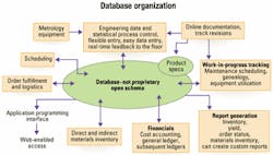
Data from each manufacturing process step, from wafer-in to package-out, is entered into the database. The steps in between include wafer processing, wafer dicing, chip testing, pigtailing, die attach, package finishing, and final packaged component test. More than 100 measurement nodes exist in the course of manufacturing each component, some of which generate tens of megabytes of test data. With thousands of parts going through a production facility, the database contains more than 3 Tbytes of information. The proper and flexible management and analysis of data are critical to maintaining and improving product performance.
When developing very complex devices, dependent on multiple variables, it is often difficult to sort cause from effect. In addition to proper design of experiments, it is necessary that data analysis be rapid and straightforward. Using the database and appropriate software, engineers can sit at their desks and correlate multiple parameters.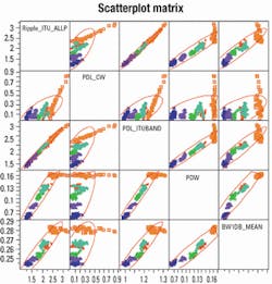
For example, Figure 3 displays a series of plots showing the interaction of several critical parameters in an AWG, such as ripple, polarization dependent loss (PDL) at the ITU grid point, PDL across the band, polarization dependent wavelength, and 1-dB bandwidth. Each of the small boxes represents a plot of interaction of two parameters, depending on the intersection of rows and columns, with different colors representing different design points. In some cases, the parameters are tightly coupled, as indicated by the diagonal lines, and in other cases the parameters are independent. With just a few keystrokes, engineers can sort through many gigabytes of information and determine the critical interaction parameters.
This process-control methodology is also critical in improving overall device performance. The final device performance can be correlated against any build parameter. For example, in the case of total isolation in an AWG, while some vendors use definitions of isolation and crosstalk that give their components the appearance of better performance, from a systems design standpoint, the important parameter is the total cumulative isolation from all other channels. That determines the total noise for which system designers must allow. When specifying a device, worst-case values must be used. The total cumulative isolation is the sum of worst-case isolation for all other channels at the worst wavelength in the passband, at worst-case polarization. That then establishes a worst-case noise value the device might exhibit. This worst-case alignment of all parameters might be statistically unlikely, but might happen, and must be guarded against.
Noise and crosstalk result from scattering of light due to imperfections in waveguides in the AWG. These imperfections cause phase errors in the light emerging from the waveguide grating which in turn cause the light to not be perfectly focused onto the proper output waveguide. These phase errors are caused by variations in the effective index, b, due to fluctuations in indices of refraction or dimensions of the grating waveguides. The total phase error is given by: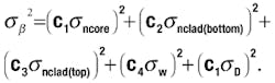
W and D represent the waveguide width and height, and n represents the indices.
The phase error from each source must be reduced to a minimum. All manufacturing processes must be highly uniform and tightly controlled to achieve high isolation. Using proper design of experiments and process control, data analysis can drive the improvement of any given performance parameter. In Figure 4, total isolation was the focus of a dedicated program to reduce the effects of all sources of noise through process improvement and control. The plot indicates total isolation in 40-channel 100-GHz AWGs over the period of one year. In this case, total isolation was improved by more than one order of magnitude from 18 to 30 dB.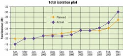
Similar development efforts have been carried out to optimize insertion loss and PDL. For example, let's look at data from an AWG with a wide band or "flat-top" passband. This device featured 40 channels with 100-GHz channel spacing. The worst-case total isolation was 28 dB, worst-case insertion loss was 5.3 dB, and worst case PDL was 0.2 dB. As always, when comparing performance numbers, great care must be taken to ensure that the same definitions are used.
AWGs represent just one building-block element that can be integrated with other building blocks to perform subsystem- and module-level functions in a single package. Other building-block functions are switches, couplers, taps, variable optical attenuators (VOAs), and splitters. Integrated components that combine 40 VOAs and a 40-channel AWG are being shipped by several vendors. This device is many times more complex than a simple AWG and represents a major step forward for optical integration.
Achieving the high performance necessary for advanced DWDM optical networks requires even more precise control of the manufacturing process. However, this level of optical integration requires only three to four mask layers and the interaction of about 1,000 optical elements-as compared to 20 mask layers-and 100 million transistors in a microprocessor. While optical integration will never approach electronic integration-since a telecommunications photon is 10,000 times larger than an electron-there is still room for progress in optical integration.
Companies around the world are working to use potential PLC functions to create integrated modules. Recent demonstrations include an integrated dynamic gain equalization chip,3 an integrated multichannel waveguide laser,4 and a frequency spectrum synthesizer.5 Such products are currently being released by several vendors and will replace rack-mounted boxes assembled out of traditional optical components. Future products will integrate multiple optical functions, including lasers, receivers, and electronics, inside one package.
AWGs perform complex filtering functions in a highly integrated and efficient way. They can replace hundreds of piece parts in conventional discrete technology. But achieving high performance requires advanced designs and precise manufacturing process control. It is possible to reliably manufacture complex PLC devices in high volumes by capitalizing on the extensive infrastructure created by the silicon IC industry. This infrastructure consists of equipment, processes, and methodologies refined over 40 years with the investment of billions of dollars. Modern database technology enables the management and analysis of the vast amount of data necessary to control manufacturing processes.
Dave Rauch is vice president of engineering at Lightwave Microsystems Corp. (San Jose, CA).
- K. Okamoto, K. Suto, H. Takahashi, and Y. Ohmori, "Fabrication of 128-chanel arrayed waveguide grating multiplexer with 25-GHz channel spacing," Electronics Letters 32 1474 (1996).
- Y. Hida, Y. Hibino, M. Itoh, A. Sugita, A. Himeno, and Y. Ohmori, "Fabrication of low-loss and polarization-insensitive 256-channel arrayed-waveguide grating with 25-GHz spacing using 1.5% D waveguides," IEEE Electronics Letters, Vol. 36, No. 9, April 27, 2000.
- B.J. Offrein, G.L. Bona, R. Germann, F. Horst, and H.W.M. Salamink, "Dyn amic Gain Equalization in High Index Contrast SiON Technology," ECOC '99 Post Deadline Papers, p. 6.
- M.W. Sckerl, S. Guldberg-Kjaer, and Chr. Laurent-Lund, "Monolithic DWDM Multi-Channel Planar Wave guide Laser," ECOC '99 Post Deadline Papers, p. 16.
- K. Okamoto, T. Kominato, H. Ya mada, and T. Goh, "Fabrication of a frequency spectrum synthesizer consisting of ar rayed waveguide grating pair and thermo-optic amplitude and phase controllers," Electronics Letters 35 (April 1999).