Vertical-cavity surface-emitting lasers break the power barrier
A new breed of semiconductor laser emerges as a promising low-cost option for long-haul data transmission.
DR. JEAN-FRANÇOIS SEURIN, TIMOTHY HAYS, and DR. L. ART D'ASARO, Princeton Optronics
Until recently, vertical-cavity surface-emitting lasers (VCSELs) have been applied primarily in short-haul data-communications networks, where these devices operate at low powers (<2 mW) and short wavelengths (around 850 nm). As a result of this early association, VCSELs gained a "low power-short wavelength" label.
However, recent technology advances have shown that VCSELs can operate at very high power and longer wavelengths, thus breaking the perceived power-wavelength barrier. These breakthroughs create a market-altering potential for VCSELs as source lasers for optical communication. Though the advances in long-wavelength VCSELs are impressive, we'll look at the more compelling aspects of high-power VCSELs and their application to tunable lasers.
To date, 850-nm VCSELs have earned a reputation as a superior technology for short-reach applications (300-500 m) such as Fibre Channel, Ethernet, and intrasystems links. Within the first two years of commercial availability (1996), VCSELs became the technology of choice for LANs, effectively displacing edge-emitter lasers. Sources emitting at 850 nm are particularly suitable for networks using multimode optical fiber.
Leveraging their success with these 850-nm devices, many VCSEL producers have now set their sites on singlemode 1,310-nm solutions. The 1,310-nm opportunity arises from the need to leverage the high-bandwidth singlemode fiber that is often already in place as well as to operate at the dispersion minimum of silica optical fiber. Given that several companies have already reported success with 1,310-nm VCSELs, it is expected that these VCSEL-based solutions will soon dominate this market segment, as well.
According to market researcher ElectroniCast, the overall market for VCSEL-based transceivers is predicted to reach $3.4 billion by 2004. The 1,310-nm very-short-reach or intrasystem link is expected to become one of the fastest-growing applications (77% per year over the next five years), reaching $900 million in 2004 and increasing to $3.7 billion in 2009. Although these links currently use edge-emitters, most analysts predict a rapid crossover to the more cost-effective 1,310-nm VCSELs as they become commercially available by the end of 2001.
Yet, the industry won't have to wait until the advent of 1,310-nm devices to reap the benefits of VCSELs in applications requiring wavelengths longer than 850 nm. Pump lasers at 980 nm show the potential of high-power VCSELs.The development of 980-nm high-power sources was initially motivated by the need for an efficient pump for erbium-doped fiber amplifiers. Although development of high-power 980-nm edge-emitters started in 1989, the first results of high-power 980-nm VCSELs weren't demonstrated until 1993, and then again, these results attracted little interest because research efforts and venture investments focused primarily on edge-emitter technology.1
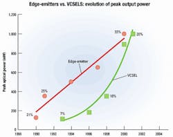
However, genuine interest in high-power 980-nm VCSELs began in 1998.2 Figure 1 shows the evolution of peak output power (at the laser facet) and corresponding wall-plug efficiency ("wall-plug efficiency" is the ratio of optical power out to electrical power in) for edge-emitters and VCSELs. It is important to note that the data shown for edge-emitters corresponds to a fraction of the results available in the literature, while the data shown for VCSELs corresponds to almost all the results available in the literature.
Today, commercially available, edge-emitter-based, 980-nm pump modules (in the standard butterfly package) demonstrate 500 mW of operating power, while in 1995, they demonstrated 100 mW. Reaching these levels of operating power has been a difficult task, and companies and universities alike have expended considerable effort to improve the reliability of edge-emitters-specifically in the area of facet passivation to minimize the effect of catastrophic optical damage (COD).
By contrast, the commercial development of high-power 980-nm VCSELs started in 1998, and pump modules operating in the 400- to 500-mW regime are already available. It is clear from Figure 1 that although little research effort was spent in the development of high-power VCSELs before 1998, improvements in the maximum achievable power and wall-plug efficiency have been exponential. Today, VCSELs are on the verge of surpassing edge-emitters in performance.
While it is true that VCSELs did benefit from some of the research done for edge-emitters, edge-emitters have two major disadvantages compared to VCSELs.
Unlike edge-emitters, where the laser output is a strongly divergent elliptical beam, VCSELs emit a uniform, circular beam, which simplifies optical system design considerably. Because edge-emitters produce an elliptical beam, the fiber coupling process is relatively complex and inefficient, where additional beam shaping components are required. Large-area, high-power VCSELs inherently emit a low-divergence, circular beam, thus facilitating more efficient coupling into a fiber or other optical components.
Edge-emitter cavities are also relatively long, typically 1 to 2 mm, and generate several longitudinal modes that cause "kinks" in the optical output power as the injection current is increased and new longitudinal modes are excited. These kinks are detrimental to the operation of the device, and the maximum operating power is limited by the occurrence of the first kink.
Conversely, the VCSEL cavity is very short compared to that of an edge-emitter. Since VCSEL cavity lengths are typically one wavelength long, only one longitudinal mode can exist, thereby suppressing the occurrence of kinks.
In terms of power, VCSEL output power scales by either increasing the aperture size of the device or arranging multiple devices in a two-dimensional array configuration. For example, VCSELs can be manufactured in arrays of 2, 4, 16, or more laser devices on the same chip. Edge-emitters aren't so nimble because increasing the aperture size has a negative influence on beam shape and coupling efficiency. Moreover, it is geometrically impractical to manufacture two-dimensional edge-emitter arrays.
The attainable optical power of edge-emitters is reaching a fundamental limit, as manufacturers are squeezing every last photon out of the structure in an effort to reach 1 W. On the other hand, the VCSEL is a very scalable structure, capable of the 1-W regime using a single device and can easily be grouped into compact arrays (<1 mm2) to produce multiwatt output levels.High-power VCSELs also offer some inherent advantages when it comes to reliability. In edge-emitters, the light is emitted over a relatively small surface, defined by the width of the contact stripe (~4 microns) and the thickness of the cavity waveguide (~1 micron), resulting in high optical power densities, which induces COD at the emission facet. Unfortunately, the thickness of the cavity waveguide cannot be increased because that would decrease the overlap between the optical intensity and the gain, resulting in poor device performance. Increasing the contact stripe width, while reducing the optical power density at the facet, increases the total number of transverse modes and results in an even more elliptical beam, which decreases the coupling efficiency into optical elements or fiber.
In contrast, the emission window of high-power VCSELs is typically on the order of 100 microns in diameter, resulting in much lower optical power densities at the emission surface, and therefore COD is not an issue in VCSELs.
The exponential improvement in achievable power for VCSELs is all the more impressive inasmuch as wall-plug efficiencies at these power levels (20% according to published material) remain well below their full potential. The wall-plug efficiency is a measure of the input electrical power converted into heat: the lower the efficiency, the more heat generated in the device. For VCSELs, the temperature rise, ΔT, in the cavity is approximately given by:where Zth is the thermal impedance, Pelectrical the injected electrical power (current times voltage), and Poptical the output optical power. The thermal impedance is approximately inversely proportional to the device diameter. Hence, high-power VCSELs with large diameters (~100 microns) have a relatively low thermal impedance.
One of the main issues in the design of high-power VCSELs is thermal management. First, the different mechanisms contributing to heat generation need to be identified and the device design optimized to minimize their effect. For example, the voltage drop across the DBRs can be reduced by introducing graded interfaces between layers. Second, efficient heat-sinking needs to be used to reduce the temperature rise in the device.
Current state-of-the-art, low-power, short-wavelength VCSELs demonstrate wall-plug efficiencies as high as 40% at operating power. High-power VCSELs are well on their way to achieving such efficiencies, and the coming years should witness a dramatic improvement in output powers.
Due to an increased demand for bandwidth, tunable lasers have recently at tracted much attention, although the idea of laser tuning has been around for many years. The applications driving the development of tunable lasers include instrumentation and system test, sparing, hot backup, fixed-wavelength laser replacement, reconfigurable optical add/drop multiplexers, optical crossconnects, and fast packet switching in the all-optical network. According to market researcher RHK Inc., the tunable-laser market is forecast to reach $1.5 billion by 2004, while it is also expected that tunable lasers will account for about one-quarter of the DWDM laser-source market by 2003. Today, several startup companies have emerged alongside more established companies with a vision of delivering an efficient, low-cost tunable-laser solution for long-haul data-communications systems.
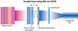
One such solution involves the use of a high-power 980-nm VCSEL (see Figure 2). In this configuration, the 980-nm VCSEL optically pumps a 15xx-nm VCSEL. Because of the lack of good semi conductor (conducting) DBRs around 1,550 nm, it is difficult to electrically pump long-wavelength VCSELs directly, and it is much more efficient to use optical pumping. The left mirror of the 15xx-nm VCSEL consists of a dielectric stack, which transmits 980-nm light and reflects 15xx-nm light. The external right mirror reflects 980-nm light and partially reflects 15xx-nm light (the rest is transmitted). Through micro-electromechanical-system (MEMS) technology, it is possible to vary the distance d between the two mirrors, thus selecting the emission wavelength.3Using an integrated approach, the 15xx-nm VCSEL can be directly bonded to the 980-nm pump VCSEL. This design considerably simplifies alignment procedures, which would be impossible using edge-emitters because additional optical components (such as cylindrical lenses) are required between the pump source and 15xx-nm active medium to reshape the elliptical output into a circular beam. In a VCSEL, the beam is already circular. Furthermore, its divergence angle is approximately inversely proportional to the beam-waist. Thus, for a large-area high-power VCSEL, for which the beam diameter is on the order of 100 microns, the beam divergence is very small (~10 degrees), resulting in a highly efficient, compact, and low-cost tunable module.
With current power levels offered by 980-nm VCSELs, 20 mW across 40 nm of tuning range can be easily obtained. As more powerful VCSELs become available, tunable lasers will scale to even higher levels of output power.
At this time, there are many well-known factors underlying the success of VCSELs in short-reach applications, and it now appears as though many of these advantages can be leveraged in the form of high-power VCSELs for use in long-haul and ultra-long-haul networks, as well. In spite of minimal funding relative to edge-emitter technology, VCSEL technology has made extraordinary progress in the areas of longer wavelengths and higher output powers. In fact, it seems evident that 980-nm VCSELs are on par with 980-nm edge-emitters in terms of output power, while at the same time demonstrating significant potential moving forward.
For skeptics of high-power VCSELs, the jury may still be out. However, within a two-year time frame, the market will ultimately dictate the future of high-power VCSELs.
Dr. Jean-FranÇois Seurin is senior device engineer, Timothy Hays is vice president of marketing, and Dr. L. Art D'Asaro is a distinguished member of technical staff with Princeton Optronics (Princeton, NJ). They can be reached via the company's Website, www.princetonoptronics.com.
- F.H. Peters, M.G. Peters, D.B. Young, J.W. Scott, B.J. Thibeault, S.W. Corzine, and L.A. Coldren, "High-power vertical-cavity surface-emitting lasers," Electronics Letters, vol. 29, no. 2, pp. 200-201, Jan uary 1993.
- R. Michalzik, M. Grabherr, and K.J. Ebeling, "High-power VCSELs: Modeling and experimental characterization," SPIE Proceedings, vol. 3286, pp. 206-219, 1998.
- D. Vakhshoori, P. Tayebati, C.-C. Lu, M. Azimi, P. Wang, J.-H. Zhou, and E. Canoglu, "2mW CW singlemode operation of a tunable 1550nm vertical cavity surface emitting laser with 50nm tuning range," Electronics Letters, vol. 35, no. 11, pp. 1-2, May 1999.
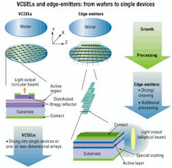
Semiconductor lasers consist of layers of semiconductor material grown on top of one another on a substrate. The grown wafer is then processed accordingly to produce individual devices.
The Figure illustrates the differences between vertical-cavity surface-emitting lasers (VCSELs) and edge-emitter structures. In a VCSEL, the active layer is sandwiched between two highly reflective mirrors (dubbed distributed Bragg reflectors, or DBRs) consisting of several layers of semiconductors. As a result, the light oscillates perpendicular to the layers and escapes through the top (or bottom) of the device.
In contrast, edge-emitters consist of cleaved bars diced from the wafers. Because of the high index of refraction contrast between air and the semiconductor material, the two cleaved facets act as mirrors. Hence, in the case of an edge-emitter, the light oscillates parallel to the layers and escapes sideways. This simple structural difference between the VCSEL and edge-emitter has important implications.
Since VCSELs are grown, processed, and tested while still in wafer form, there is significant economy of scale resulting from the ability to conduct parallel device processing, whereby equipment utilization and yields are maximized and set up times and labor content are minimized. In the case of a VCSEL (see Figure), the mirrors and active region are sequentially stacked along the y-axis during epitaxial growth. The VCSEL wafer then goes through etching and metalization steps to form the electrical contacts. At this point, the wafer goes to test where individual laser devices are characterized on a pass-fail basis. Finally, the wafer is diced and the lasers are binned for either higher-level assembly (typically >95%) or scrap (typically <5%).In a simple Fabry-Pérot edge-emitter, the growth process also occurs along the y-axis, but only to create the active region as mirror coatings are later applied along the z-axis. After epitaxial growth, the wafer goes through the metalization step and is subsequently cleaved along the x-axis, forming a series of wafer strips. The wafer strips are then stacked and mounted into a coating fixture. The z-axis edges of the wafer strips are then coated to form the device mirrors. Now, the wafer strips are diced to form discrete laser chips, which are then mounted onto carriers. Finally, the laser devices go into test.
It is also important to understand that VCSELs consume less material: In the case of a 3-inch wafer, a laser manufacturer can build about 15,000 VCSELs versus approximately 4,000 edge-emitters.
In addition to these advantages, VCSELs also demonstrate excellent dynamic performance such as low threshold current (a few micro-amps), low-noise operation, and high-speed digital modulation (10 Gbits/sec). Furthermore, although VCSELs have been confined to low-power applications-a few milliwatts at most-they have the inherent potential of producing very high powers.


