Integration of multifunctional planar lightwave circuits
With the right technological approach, planar lightwave circuits can address a variety of applications.
DR. ANTHONY TICKNOR, Lightwave Microsystems
The management of exponentially growing Internet traffic, coupled with the deployment of DWDM systems to meet that growth, has changed the face and future of the optical network. Triple-digit collections of multigigahertz channels are to be routinely squeezed into fiber cores a few microns wide and retain complete individuality. With such soaring network complexity, network systems integrators seek further integration of functionality within the optical components they use. That has created an unprecedented surge of new-product development for fiber-optic-network components.
One technology that can aggressively address the increasing need for integration is currently being used to make planar lightwave circuits (PLCs). By using manufacturing techniques closely related to those employed for silicon integrated circuits, a variety of optical circuit elements can be placed and interconnected on the surface of a silicon wafer or similar substrate. This technology has only recently emerged and is advancing rapidly with leverage from the more mature tools of the semiconductor-processing industry.
Currently, the predominant commercial application of PLC technology is for making arrayed-waveguide gratings (AWGs) for multiplexing and demultiplexing multiple wavelengths in a DWDM system. Although generally perceived as a single-function device, such an application can perform the function of more than 100 discrete fiber-optic components1 and already represents a considerable degree of integration. Furthermore, programmable functions such as variable optical attenuators (VOAs) and switches made with compatible PLC technology are now moving into commercial production.The primary commercial technology for integrating these programmable functions on PLCs is thermo-optic. Recent demonstrations of electro-optic and micro-electromechanical systems (MEMS) devices are also notable. On the horizon are other possible technologies for dynamic functions, including acousto-optic, elasto-optic, and photo-refractive.
In the near term, thermo-optic technology will provide most of the active functions in PLCs that combine multiple functions. Thermo-optic devices are directly integrable in waveguide form and can provide a uniform response to the randomly varying polarization of the optical signal presented by the telecommunications network.
Research is also progressing to develop compatible technologies for the integration of other basic functions such as waveguide amplifiers, tunable filters, circulators, and other functional configurations. Clearly, a primary strength of PLC technology is how directly it lends itself to integrating diverse functions into complex optical circuits. There have already been suggestions and reports of prototypes for cascading switches or VOAs with multiplexers or demultiplexers to make add/drop multiplexers and programmable filters.2,3 It is easy to foresee in the not-too-distant future network nodes that have as their optical "hearts" one or two network-on-a-chip components buried inconspicuously away, pumping data streams among a multitude of ports in response to the dynamic demands of the embedding network.
Properly fabricated PLC waveguides based on silica glass (SG) and doped silica glass (xSG) have superior loss characteristics for transporting the optical signals used in telecom networks. They also have relatively little sensitivity to changes in ambient temperature. (However, sophisticated devices such as the AWG filter are sensitive even at this low level and must be thermally stabilized or made with specifically reduced sensitivity.)Where strong, highly localized index gradients are not achievable, programmable devices must typically rely on multipath interference. The optical signal is split into two or more optical signals traveling along separate optical paths. The paths must diverge to at least a separation of tens of microns so thermo-optic refractive-index changes may be applied to one path independently of the other. The signals must then be suitably recombined to provide the desired total response. The fine detailed shape and index distributions of each path will determine the relative phases accumulated by the optical signals in each separate path.
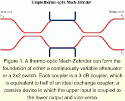
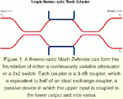
A simple interferometer, the 2x2 Mach-Zehnder, with integrated heaters over one or both arms, is depicted schematically in Figure 1. This device can be fabricated to make either a continuously variable attenuator or a 2x2 switch. Each coupler is a 3-dB coupler, which is equivalent to half of an ideal exchange coupler, that being a passive device in which the upper input is coupled to the lower output and vice-versa.
Optical signals entering the device at the upper input port, Pin, are divided in the first 3-dB coupler region. This division sends half the power through the upper arm and half through the lower arm, but the half in the upper arm lags the half in the lower arm by one-quarter of a wavelength of the optical carrier. With no thermal input in an ideal device, the two halves of the signal converge on the second 3-dB coupler region, with the half in the lower arm having the same one-quarter-wave lead. It is as though the arms are not there and the exchange coupling is completed in the second 3-dB coupler region and the signal exits from port P3.
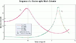
Suppose instead that power is applied to the electrode overlaying the lower arm such that the index of refraction for that arm increases enough to delay the half of the signal traveling in that arm by half of a wave. In that instance, the two halves of the signal converge on the second coupling region with the half in the upper arm leading by one-quarter wave. This is the top-to-bottom mirror image of the unpowered state. Hence by symmetry, the exchange coupling is reversed and the signal from Pin exits from the directly opposing output port, P2. Drive levels producing delays other than integer multiples of one-half wave lead to intermediate coupling conditions with the input signal divided fractionally between the two outputs.The thermo-optic response of an all-silica device of the type depicted in Figure 1 is shown in Figure 2. This particular device was not made with equal-length paths, and the zero-power state is not the crossover state. This response shows that as the drive voltage on one heater increases toward 4 V, all the input light is directed into output arm P2 and output from P3 is extinguished. As the drive voltage is further increased toward 10 V, the light is switched out of P2 and into P3.
This device was designed to be a programmable attenuator for the P2 output. If this design were used as a switch, the response curve shows that the isolation of the dark output would be very sensitive to precise control of the thermal input.
Research demonstrations of complex multifunction devices monolithically integrated on the same substrate have already been reported.4,5 Among the first multifunction PLCs likely to see widespread use is the cascade of a high-performance AWG filter with an array of thermo-optic VOAs for balancing the power levels among the individual channels. The primary use of such a device is to pre-distort the amplitude spectrum to better distribute the composite amplifier gain on a channel-by-channel basis.The engineering challenges for manufacturing usable devices in such configurations are substantial. In particular, thermal management presents a notable contradiction. Although athermal AWG technologies are currently being investigated, high-performance, reliable examples of such elements are not yet ready for production. Lacking an athermal AWG, it is required to provide a tightly limited, stable, and uniform temperature across the grating region of the AWG. This factor dictates a preference for the PLC to be thermally insulated from the uncontrolled environment.
Meanwhile, elsewhere on the PLC within the array of VOAs, varying levels of power are being dissipated, perhaps reaching levels of several watts in some instances. That dictates a preference that the PLC have aggressive heat-sinking to prevent excessive heating. Balancing these opposing demands is one of the key engineering issues for realizing robust high-performance, multi function components.
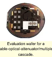
An engineering evaluation chip containing a single 40-channel VOA-array/multiplexer cascade is shown in the photo on page 226. The AWG can be seen clearly in the upper section of the device. Below that is a bright area resembling a block letter "P." This area is the set of metal traces connecting the heater electrodes to the bonding pads near the bottom of the device. Due to the high density of metal lines, the individual lines are not resolved in this picture except very near the heater electrodes.
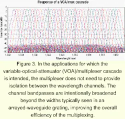
The output of the multiplexer is routed back near the device input to facilitate testing prototypes of different sizes. Figure 3 shows the multiplexer behavior of a pre-production prototype VOA/ multiplexer. In the applications for which this device is intended, the multiplexer does not need to provide isolation between the wavelength channels. The channel bandpasses are intentionally broadened beyond the widths typically seen in an AWG, improving the overall efficiency of the multiplexing.The engineering of these devices will provide much of the foundation for the coming generation of components that will provide higher-level optical functions. Expect to see programmable-amplitude optical filters for inline gain-profile compensation at a similar level of integration. These devices divide an optical spectrum into multiple bands, apply VOAs to set distinctive transmission levels for each of the bands, then recombine the bands. Some of these inline filters will use a discrete set of bands matched to the DWDM channels of the system for channel-power balancing. Others will use an overlapping set not necessarily matched to the channel grid to make a spectrally continuous filter function not sensitive to the actual channel configuration within it's spectral domain. The same principle can also be used to provide minor adjustments to the time delay rather than transmission of the bands to make a dynamic dispersion compensator.
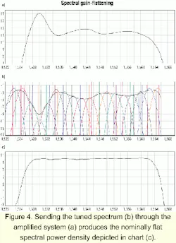
Figure 4 displays the use of a programmable filter for simple gain-curve compensation. Chart (a) shows a hypothetical composite gain curve for a system. Chart (b) shows an 18-channel overlapping filter where the transmission levels of the individual channels can be programmed to produce a composite transmission curve (herein black) that is the approximate inverse of the gain curve. Sending the tuned spectrum (b) through the amplified system (a) produces the nominally flat spectral power density depicted in chart (c).
At a similar level of functional density is the fully integrated reconfigurable optical add/drop multiplexers. Recon figurable devices accessing 40 or 80 channels or more will become available with the growth of engineering and manufacturing experience.
The history of PLCs has strong roots in polymers as well as inorganic waveguides. The first commercially produced solid-state fiber-optic switches were based on polymer PLCs,6 and more complex devices continue to be demonstrated in polymer waveguides.7 Optical polymers tend to have thermo-optic coefficients an order of magnitude larger than silica while possessing a thermal conductivity that is an order of magnitude less. That enables much larger thermally generated index gradients to be produced in all-polymer waveguide structures compared to silica waveguides. These stronger gradients enable the design of switching and attenuation elements that can function more robustly than silica thermo-optic components and require lower power.
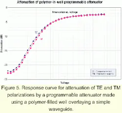
But although optical polymers may be able to get loss rates down to a few tenths of a decibel/centimeter, that is still generally too high for practical use as the basic waveguide structure in a complex PLC. What's desired is the integration of both silica and polymer waveguides on the same substrate to realize multifunction waveguide devices with the beneficial properties of both silica and polymer waveguides as appropriate.The first series of hybrid silica/polymer devices has been investigated and were made by removing some of the top cladding to within a few microns of the waveguide core and replacing it with an optical polymer. The optical polymer was designed to have an index value near that of the silica core near room temperature and more near the cladding index at elevated temperature. When the polymer is heated, the polymer in the well is of lower index and behaves as cladding and light propagates through the core with little loss. As the heat is turned off and the temperature is allowed to drop, the index of the polymer rises and the mode begins to leak into the polymer in the well. As the temperature of the well cools to that of the substrate, the mode becomes very "lossy" and the device exhibits strong attenuation. Such a device can be easily used as a programmable attenuator. Figure 5 shows the data of a typical attenuation response for such a device.
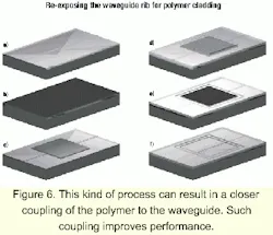
Further improvements can be made by more closely coupling the polymer to the waveguide. One approach for realizing such a configuration is depicted in Figure 6. Starting with the patterned ribs of core silica (a), the wafer is coated with a material that can tolerate subsequent silica processing steps but can also be selectively removed at a later time (b). This material could be, for instance, amorphous silicon (a-Si). This coating is then removed everywhere except in the regions where the thermo-optic structures are to be formed (c). The whole wafer is then coated and processed for the upper-cladding silica layers (d).
When the silica processing is completed, the areas of a-Si are exposed (e) and can then be selectively removed, e.g., with a XeF2 etch, leaving the original silica core ribs exposed in the active area (f). The re-exposed rib can now have polymer coated directly onto the waveguide core only in the exposed region.
These polymer-coated singlemode silica ribs have a subtle thermo-optic behavior. Typically, for such structures, 85%-95% of the optical field is in silica and the remaining fraction is in polymer. However, the polymer has a thermo-optic response 10-20 times greater in magnitude and of opposite sign than the silica. Because of these relationships, uniform changes in temperature have little effect on the propagation constant of a mode through the polymer-clad silica. That is to say, the effective index of the mode actually has a reduced response to a uniform change in temperature as compared to the all-silica waveguide. In fact, the structure can be designed to have nearly zero thermo-optic response a round some operating temperature.
Such a configuration used in the grating of an AWG can enable significant relaxation of the thermal-stabilization requirements for the filter. When highly localized heating is applied to the polymer-coated ribs, a significant thermo-optic response is still realized due to the much higher thermal resistance of the polymer than that of the silica or silicon. When a heater is operated on the upper surface of the polymer, most of the temperature drop occurs across the polymer layer while the substrate remains near the ambient temperature. The structure does not see a uniform temperature change, but rather a thermal gradient in the polymer cladding.
This effect works with the thermo-optic response of the polymer to induce the desired changes in the propagation constant of the mode in the waveguide with respect to neighboring waveguide modes, and consequently robust thermo-optic devices can be made. The thermo-optic response of such a waveguide is less than that in an all-polymer segment, and as such, polymer-clad rib devices must be somewhat longer than all-polymer de vices. But since the larger fraction of the optical field is in silica, these devices have lower loss rates than all-polymer segments, and due to the guaranteed alignment and continuity of the geometry, the device can exhibit less total loss than its shorter all-polymer counterpart.
Incorporation of optical polymer may be used to either reduce the temperature-stability requirements of the filters, reduce the power consumption of the programmable functions, or both. In addition, the stronger thermal-index gradients possible in polymer waveguides enable a class of switches known as digital optical switches that have certain desirable operating characteristics over interferometric thermo-optic switches. By accommodating integration with silica-waveguide technology, polymer waveguides should continue to play an important role in the future of PLCs.
The realization of optical integration is frequently compared to the rise of the silicon integrated circuit. There are many apt analogies, some due to natural technology similarities and others imposed by the use of silicon technology as a model and toolset. Yet, PLC technology will also have distinctive characteristics of its own. The use of highly nonlinear optical functions is not yet apparent, and there is no foreseeable way to confine photons down into the ultra-small volumes in which electrons can be controlled. Hence, optical elements can be as thin as a few microns but are likely to remain millimeters long or longer. That means we are never likely to see millions of optical-waveguide elements arrayed across the surface of a PLC like the transistors on an IC.
On the other hand, many of the optical elements are perfectly happy sharing real estate with other independent optical elements in the same layer. Furthermore, overlaying waveguides on multiple layers also is quite possible. In the highly functional PLCs of the future, many different functional units may be sharing the same chip area. Conventional microscopic imaging of such a chip would not reveal the well-defined structures and functional-unit areas along a rectilinear grid that is so familiar in silicon ICs.
The image of such a chip surface would more resemble a confusing multiple exposure of sweeping elements along a variety of orientations. Future products will further integrate these and other contrasting technologies into multiple optical functions, including lasers, amplifiers, ultra-fast switches, receivers, and electronics, on the device.
Dr. Anthony Ticknor is director of research and development at Lightwave Microsystems (San Jose, CA). He can be reached at [email protected].
- J. Lam and L. Zhao, "Optical Integration is Rising to Meet Growing Bandwidth Demand," Laser Focus World WDM Solutions, October 2000, p. 25.
- K. Okamoto et al., "16-Channel Optical Add/Drop Multiplexer Consisting of Arrayed-Waveguide Gratings and Double-Gate Switches," IEEE Electronics Letters 32, 1471 (1996).
- C.K. Madsen and J.H. Zhao, "A General Planar Waveguide Autoregressive Opti cal Filter," IEEE Journal of Lightwave Technology 14, 437 (1996).
- C.R. Doerr et al., "Dynamic Wave length Equalizer in Silica Using the Single-Filtered-Arm Interfero meter," IEEE Photonics Technology Letters 11, 581 (1999).
- A. Ticknor and K. Purchase, "Inte grated Switches for Recon figurable Optical Add-Drop Modules," SPIE Conference #3949 proceedings, Photonics West 2000.
- Akzo Nobel, BeamBox product, JDS Uniphase.
- G. Beelen et al., "First Polymer Based Reconfigurable Add-Drop Multi plex er," ECOC '99 Post Deadline Papers, p. 58.
