New research bolsters development of 1,300-nm VCSELs
By MEGHAN FULLER
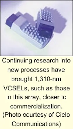
Vertical-cavity surface-emitting lasers (VCSELs) have displaced their edge-emitting counterparts in the short-wavelength or 850-nm window, and many in the industry believe they will have a similar impact at 1,300 nm. To date, manufacturing challenges have prevented the widespread deployment of VCSELs at this wavelength. However, three papers presented at the Conference on Lasers and Electro-Optics (CLEO 2001-Baltimore) indicate that 1,300-nm or 1.3-micron VCSELs are approaching commercial viability for optical component and subsystem applications.
VCSELs are constructed by sandwiching an active region or gain medium between layers of crystals that act as mirrors. The gain medium and mirrors of 850-nm VCSELs are made from the same material, a compound of gallium and arsenic (GaAs), which enables manufacturers to grow both in one relatively simple process known as molecular-beam epitaxy (MBE). VCSEL gain media in the 1,300- and 1,500-nm window, by contrast, are grown from a different material, indium phosphide (InP). Manufacturers have been unable to develop a single epitaxial process for these VCSELs, because mirrors are extremely difficult to construct from InP.
MBE works on the principle of thermal evaporation. In 850-nm VCSEL production, the GaAs substrate sits in a vacuum chamber above separate heated crucibles for each of the materials that will eventually compose the gain medium and mirrors-gallium, aluminum, arsenic, nitride, indium, etc. When the elements are heated, they evaporate as a collimated beam of material that then arrange themselves in layers on the surface of the substrate.
Critical to MBE is the process of lattice matching. As layer after layer of the elements hit the substrate, the lattices or crystals must have the same dimensions, or defects will form in the mirror. The lattice mismatch of InP is such that the Bragg mirrors do not work efficiently enough to make 1,300-nm VCSELs a viable option for long-wavelength applications.
Researchers from Bell Labs, Lucent Technologies (Holmdel, NJ) believe they may have devised a solution to the lattice mismatch problem that would enable them to use a single epitaxial process for 1.3-micron VCSELs. Their study, "Room Temperature CW Operation of GaAsSb/GaAs VCSELs near 1.3 Microns," explores the feasibility of continuous-wave (CW)-operated VCSELs using epitaxy technology on GaAs.
They used a nonconventional GaAs-based material known as gallium arsenide antimony (GaAsSb) instead of InP, which enabled them to construct a 1.3-micron VCSEL using MBE. "Our efforts have been mostly concentrated on epitaxial growth on GaAs substrates of GaAsSb quantum wells with 30% antimony refraction, which emit near 1.3 microns, and optically pumped VCSELs with such GaAsSb wells," explains Dr. Francesco Quochi, post-doctoral fellow at Bell Labs.Researchers at Sandia National Laboratories (Albuquerque, NM), in conjunction with the Department of Electrical and Computer Engineering at the University of Illinois (Urbana), also looked at the feasibility of using different elements to create long-wavelength VCSELs. "We are currently pursuing mainly the quaternary material InGaAsN [indium gallium arsenide nitride]," explains Hans Christian Schneider, one author of the paper, "because this is the most promising approach that makes use of existing techniques to fabricate the laser mirrors." They were successful in their efforts to grow the entire laser structure-including the active region, cavity, and mirrors-by MBE.
The Sandia Labs study, entitled "Temperature Dependence of Threshold Current in a 1.3-micron InGaAsN VCSEL: Theory and Experiment," also examined the dependence of threshold current on temperature for InGaAsN/GaAs VCSELs, which has been another big hurdle in the development of long-wavelength lasers. "One question concerning the applicability of such a device is the sensitivity of laser performance to temperature variations," explains the report.
Pulsed VCSELs, used in non-telecommunications applications, are relatively easy to manufacture. The current is sent through the VCSEL in very quick bursts or pulses to allow the heat to dissipate. The problem with pulsed VCSELs, explains Dr. Ryan Naone, VCSEL device engineer at Cielo Communications (Broomfield, CO), is that many telecom applications require a wide temperature range of 40 to 85°C. "You can't use [a pulsed] VCSEL for communications purposes because you have a laser power that is turning off and on. Continuous wave means that current is constantly flowing through the VCSEL; you can have the current on 100% of the time and it's a useful transmitter."
Schneider and others demonstrated 1.3-micron operation of an InGaAsN VCSEL over the temperature range of 270° to 350°K. "The threshold current variation over this range is less than 20%," concludes the report. CW operation over a range of temperatures will enable 1,300-nm VCSELs to compete with existing edge emitters, including Fabry-Perot and uncooled distributed-feedback lasers.
Cielo Communications also presented a paper-in collaboration with Sandia Labs-in which they too explored the use of InGaAsN for 1.3-micron VCSELs. Entitled "1.3-micron InGaAsN VCSELs on GaAs Substrates," the Cielo study also proved that such a VCSEL could be grown by MBE and achieve CW room temperature lasing. The importance of the findings, claims Naone, "is the fact that it's going 10 Gbits/sec, which enables it to be compliant with OC-192 and SONET-and every speed lower than that."
The real significance of these advancements also can be seen on a component level or an optical subsystem level, he contends. In the past, the only viable laser sources available were either Fabry-Perot or distributed-feedback lasers, which require more energy, give off more heat, and necessitate coupling optics because they have a very elliptical beam pattern that does not fit well into singlemode fiber.
"We really see the 1,300-nm VCSEL as enabling fiber optics to reach the next generation, because you can do things from a cost and performance side that you could never in a million years be able to do with an edge emitter," says Naone. Such applications include fiber-to-the-home and two-dimensional arrays for micro-electrical mechanical systems (MEMS).
Bell Labs' Quochi agrees. "Monolithically grown 1.3-micron VCSELs represent an attractive, cost-effective solution for metropolitan optical communications and optical interconnects," he says.
Stephen Montgomery, president of the market researcher ElectroniCast Corp. (San Mateo, CA), is quick to point out that "not everything is going to be VCSELs," however. A recent ElectroniCast study indicates that 1,300-nm VCSELs may not displace their edge-emitting cousins for quite some time.
"Within the 10-Gbit/sec serial market," says Montgomery, "we believe 100% of the 1,310-nm [segment] will be edge emitters in 2001. However, by the year 2010, 53% of all transceivers will be 1,310-nm VCSELs. They will start taking over at 10 Gbits/sec and later on some other data rates basically because they are more cost-effective."
Cielo Communications (Broomfield, CO) has moved the InGaAsN technology discussed in the main article from the laboratory to the field with the introduction of a pair of 1,300-nm VCSEL-based devices.
The company has launched a 2.5-Gbit/sec, 1,310-nm parallel array module available in eight-fiber and 12-fiber versions. Mick Wilcox, product marketing engineer at Cielo, says he expects the eight-fiber version to find favor in front-panel applications for SONET/SDH environments, including switches, crossconnects, muliplexers, and other transport equipment. Backplanes form the target application for the 12-fiber module, an application that Wilcox expects will take off first.
The arrays feature directly modulated operation, a small footprint similar to current 850-nm devices, power consumption of 2 and 3 W (respectively), and a 3-dB additional power budget over typical SONET/SDH 2.5-Gbit/sec specifications. The additional power supports transmission distances of up to 15 km.
Meanwhile, Cielo has also introduced a 10-Gbit/sec serial transponder based on the same 1,310-nm technology. Jeff Bisburg, Cielo's product marketing manager, expects the device to play in SONET/SDH and 10-Gigabit Ethernet applications, particularly for switches, routers, add/drop multiplexers, DWDM terminals, and multiservice platforms.
A limited number of users interested in nonstandard optical backplane designs may also find the device appealing, he says.
The transponder requires 3 W of power and takes up 1.66x3x0.5 inches of space, the same footprint as similar 850-nm devices, using a 200-pin format. It will support 10-km 10-Gigabit Ethernet applications as well as similar distances for other uses in the SONET/SDH, Fibre Channel, or Optical Internetworking Forum spaces.
Both devices should be available in sample quantities this summer, with production beginning this fall.
- Stephen Hardy

