Adjusting APD power-supply voltage with DACs and variable resistors
by James Horste
Avalanche photodiodes (APDs) are used as receiving detectors in optical communications systems. APDs operate with a reverse bias voltage across the junction that enables the creation of electron-hole pairs in response to incident radiation. The electron-hole pairs are then swept by the applied field and converted to a current that is proportional to the radiation intensity.
To get the ultimate sensitivity out of these devices the reverse voltage needs to be as high as possible without hitting the breakdown voltage. Breakdown would cause excessive current to flow through the junction. If this current isn’t limited it could destroy the APD.
APDs are frequently operated at 90% of breakdown voltage or even higher. The breakdown voltage can vary from part to part and will also vary with temperature. To safely use an APD with these high biases the power supply voltage must be set and maintained at a safe value for the particular APD used in the system. In high-performance systems the voltage will also need to be varied with temperature.
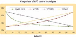
There are several options for adjusting the power supply voltage. The most common are variable resistors, potentiometers, voltage output digital-to-analog converters (DACs), and current output DACs. Each of these parts has a different response when used to control a power supply. Figure 1 shows how APD voltage would vary when controlled by each of these options. Each approach has different advantages and disadvantages, which this article will review.
The terms “variable resistor” and “potentiometer” are frequently used interchangeably. For this article, a variable resistor will be defined as a two-terminal device with a variable resistance between the terminals. A potentiometer will be a three-terminal device with a fixed resistance between two of the terminals and a third terminal called the wiper.
Variable resistors come in several types. Mechanical variable resistors are common; however, to avoid the labor of setting a resistance value with a knob or set-screw, digital variable resistors perform the same functions but replace the mechanical adjustment with a simple two-wire serial interface such as I2C. These digitally controlled resistors, though, don’t offer the smooth analog adjustment range that a mechanical wiper permits. Rather, the maximum resistance setting, Rmax, is divided into n increments (typically 32, 64, 128, or 256 taps) and data sent to the I2C control port tells the resistor how many taps to concatenate to set the resistance value.
Rsetting = Rmax/n × T (the number of taps selected)
The larger the number of taps, the smaller the resistance increment for each tap, and thus the more precisely the value can be set to the desired resistance. Dual temperature-controlled nonvolatile resistors that combine a pair of variable resistors (for example, a pair of 10-kΩ resistors or a 10-kΩ and a 50-kΩ) also are commercially available.
When used to control a power supply, variable resistors feature negative slope and nonlinear performance. The fact that resistor divider values can be scaled up or down to optimize power supply design is one advantage they offer. Variable resistors also only take up two pins on a system chip and don’t require any voltage references. This makes them popular choices for inclusion on fiber-optic control circuits.
However, the negative slope means the system must be powered up with resistance at maximum value to guarantee minimum APD voltage. Nonlinearity must be considered in temperature-compensation systems.
The potentiometer is best understood by considering the mechanical version. There are two terminals with a fixed resistance between them. The third terminal is called a wiper and moves up and down the fixed resistor. The electronic version uses switches (taps) to approximate the function of the wiper. Where the mechanical pot has near infinite resolution, the resolution of the electronic version is determined by the number of switches used-just like in the previous example of the variable resistor.
If only the wiper and one of the other terminals are used, then the potentiometer can be used as a variable resistance. The advantage of the potentiometer is the voltage at the wiper is a fraction of the total voltage across the total resistance. Assuming a linear taper, the voltage at the wiper is directly proportional to wiper position. If the voltage at the wiper is buffered, the potentiometer can be thought of as a voltage-output DAC (which is described in the next section). If the wiper is not buffered, the total impedance seen through the wiper will vary from R/2 at the midpoint to a very low value at the extremes. This change in resistance will contribute to nonlinearity when used with other fixed resistors.
When used to control a power supply, potentiometers exhibit positive or negative slope depending on the connection of the part. For example, they can be set up for positive slope so the APD voltage will start at minimum at turn-on. Potentiometers also provide more linear response than variable resistors. They also don’t need a reference voltage.
On the other hand, the potentiometer resistance determines the resistor divider values. Thus, a high-value potentiometer forces the use of high-value resistor dividers, which may cause errors due to leakage currents in the feedback path. Potentiometers also require three pins on system chips.
The voltage-output DAC is the most common type of DAC. It can take many forms: the potentiometer with a buffer on the wiper output as described previously; a microcontroller with a pulse-width-modulated (PWM) squarewave output and filter; or a dedicated DAC IC that could integrate one or more DACs.
Voltage-output DACs enable resistor values to be scaled up or down to optimize power supply design. Many systems have some form of voltage DAC output available. These DACs also provide linear response.
However, their negative slope means the system must be powered up with voltage at maximum value to guarantee minimum APD voltage. They also require a voltage reference.
The current-output DAC is becoming more popular in fiber systems. The current output is set up as a sink so it can be easily interfaced to current-mirror type laser controllers. With the increased popularity of these DACs it becomes more likely that a spare DAC section may be available for APD control.
Many systems have some form of current-sink DAC output available. These DACs offer linear response; their positive slope means APD voltage will start at minimum at turn-on. Disadvantages include the fact that the DAC sink-current range fixes resistor divider values. High DAC currents mean high APD currents. These DACs also require a reference. Overall, the current-sink DAC is not as common as the other options yet.
Current-source DACs are not appropriate for fiber applications and will generally not be available in small packages. They will not be discussed here.
Not surprisingly, which option will work best in a particular application depends on a variety of factors. For example, available parts: One of the options mentioned may already be in use in the system and have spare control outputs. Examples would be a microcontroller with spare PWM DAC outputs or laser controllers with spare variable resistor outputs.
If it is necessary to do temperature compensation then the resolution of the APD control circuit must be considered. You need to make sure the section of the response with the worst linearity will still give the necessary resolution.
You also have to make sure that the system will start up at a safe voltage. Here are some options:
- Keep the power supply off until the correct value is loaded into the control device.
- If a nonvolatile device is used that will power up with the previous commanded value, that may be good enough. The danger is if the system powers down at one temperature then powers up at another, the new voltage may be too high.
- Make sure control powers up at an output that gives minimum APD voltage.
If a PWM with a filter is used as a voltage-output DAC, make sure that the filter settling time is considered. The filter output will start at zero and ramp up, which means the APD voltage will start at maximum and ramp down.
Resistor divider resistance must be high enough to minimize current draw but low enough so currents on the feedback node don’t cause errors.
Finally, the amount of adjustment range will depend on several factors. The adjustment range must accommodate the production variation of the photodiodes and also the variation with temperature. Some designers use the same circuits for both long-reach and short-reach systems, changing the optics and APD as appropriate. These systems will require much larger adjustment ranges.
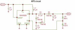
Figure 2 shows an example of a 70-V APD power supply using a PWM step-up DC-DC converter. The lateral DMOS switching MOSFET inside the IC is rated at 40 V maximum so the switcher is operated at 35 V and a voltage doubler circuit is added to the output to get to 70 V. The voltage doubler consists of C2, C3, D1, and D2. If no more than 35 V are required, then these parts can be omitted.
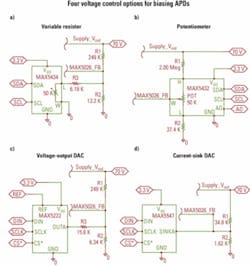
Let’s now examine a few different configurations of power supplies and the related design equations for circuits controlled by a variable resistor, a potentiometer, a voltage-output DAC, and a current-sink DAC (Fig. 3a, b, c, and d, respectively). All examples have an output range of 30 to 70 V and use a reference voltage of 1.25 V. The design equations can also be applied to any power supply with an external feedback divider.
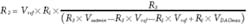
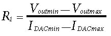
Variable resistor design equations: For the variable resistor design approach shown in Fig. 3a, the output voltage is controlled using a variable resistor and can be calculated as follows:
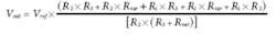
The desired output voltage range spans Voutmin = 30 V to Voutmax = 70 V and the variable resistor resistance range goes from Rvarmin = 610 Ω to Rvarmax = 50 kΩ. Thus, the Voutdelta = Voutmax - Voutmin = 40 V.
Next, select the value for R1, R1 = 249 kΩ, and then calculate the values of R2 and R3:
R2 = 13.41 kΩ (13.3 kΩ is the closest standard value)

R3= 6.234 kΩ (6.19 kΩ standard value)
Potentiometer design equations: In the potentiometer-based design example shown in Fig. 3b, a potentiometer replaces the variable resistor. The values can be calculated as follows:
Equation for the output voltage, with X = the wiper position, 1 = top and 0 = bottom is:
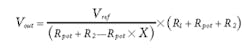
The desired output voltage range is Voutmin = 30 V to Voutmax = 70 V and the potentiometer end-to-end resistance (Rpot) is 50 kΩ. Now you can calculate the values of R1and R2 as follows:
R1 = 2.013 MΩ (2 MΩ is the closest standard value)
R2 = 37.5 kΩ (37.4 kΩ is the closest standard value)
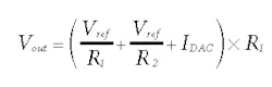
Voltage-output DAC design equations: When the design uses the voltage-output DAC, as shown in Fig. 3c, the APD output voltage is controlled by the voltage-output DAC. The APD output voltage can be calculated as follows:
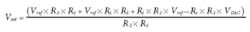
The desired output voltage range spans Voutmin = 30 V to Voutmax = 70 V, with a DAC range of VDACmin = 0 V to VDACmax = 2.5 V.
Next, select a value for R1. Use 249 kΩ as an example, and now the values for R2 and R3 can be calculated as follows:
R2 = 6.385 kΩ (6.34 kΩ is the closest standard value)
R3 = 15.56 kΩ (15.8 kΩ is the closest standard value)
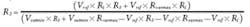
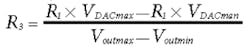
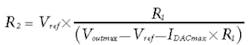
Current-sink DAC design equations: When a current-sink DAC is used rather than the voltage-output DAC, as shown in Fig. 3d, the equation to determine the output voltage becomes:
The desired output voltage range spans Voutmin = 30 V to Voutmax = 70 V, and the current-sink DAC range spans IDACmin = 50 µA to IDACmax = 1.2 mA. Thus the values of R1 and R2 can be calculated as follows:
R1 = 34.78 kΩ (34.8 kΩ is the closest standard value)
James Horste joined Maxim Integrated Products (www.maxim-ic.com) in 1999 as a field applications engineer and was promoted to field applications training in 2005. He earned a BS in electrical engineering and computer engineering from the University of Michigan in 1983.