Importance of robust closed loop control for components
With the downturn in the telecommunications business, most of the leading edge optical-component activity today occurs in very young companies, with major suppliers willing to take a wait and see attitude as they struggle to survive through the slump. Key to these developments is new research in device physics and materials. The real challenge is the optics: how to bend light, switch light, create coherent light at specific wavelengths and multiplex channels to operate over a single fiber and over long distances with minimal optical loss.
However, without the associated electronics, these devices are useless, and next-generation optical components such as dynamically and widely tunable laser sources require sophisticated electronics. The electronics control such device performance attributes as noise, the bandwidth of the current loops, the linearity of voltage drivers, the precision associated with temperature control, and the overall closed loop control laws. This type of electronics design requires a different skill set from optics altogether. And systems integrators of optical technology can be expected to demand complete solutions from optical-component suppliers that combine leading edge optics, embedded controls, and in some cases payload-aware communications electronics, tightly integrated into a complete solution.
So then, what is the problem?
Advanced optical components frequently are not easily made "plug and play" to their system environment or their controller host; there are few industry standards on technologies and interfaces to simplify the complexity. That means with each new optical discovery, a new and unique control system must be designed.
Optical devices require multiple levels of control. In its simplest form, a single feedback element drives a single control element. But in most applications, to compensate for aging effects and nonlinearities, a simple solution will not provide the robustness needed.
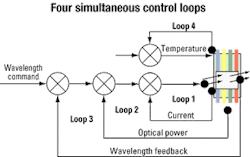
For example, in applications like an optical-crossconnect switch, the optical device must be able to manage the switching of light from any input port to any output port. The device must ensure that the light intensity is within the specified margin with the degree of stability and control necessary for reliable operation. Just in this simple example, it is conceivable to have four simultaneous control loops (see Figure 1), including an outer loop measuring overall wavelength feedback and providing management of the device, a loop to ensure the intensity of the light is properly directed, an inner current loop for stability, and a fourth loop controlling temperature. So there are four signals for control of a single optical device. How to decide which feedback takes a higher priority or which characteristic is more important? Additionally, there are many dynamic factors to consider:
- Short-term stability. How fast can the system stabilize its output relative to the small changes in a commanded set point or a small environmental disturbance?
- Long-term stability. How the system's performance changes over time due to aging effects in either the optics or the electronics.
- Reliability. How long the system can be expected to operate at the acceptable performance range.
- Large-signal dynamic response. How fast can a system respond to a step change in commanded set point or a large environmental disturbance?
Often, well-established single input, single output (SISO) control techniques such as proportional, integral differential (PID) or proportional, integral (PI) can be used as "control building blocks" and combined in creative topologies such as cascaded loops to achieve the desired closed-loop-system response. In a typical cascaded system, the inner control loops have the fastest performance and are used to "linearize" a particular low-level-state variable such as the current applied to a Bragg grating. Outer control loops are typically slower and are used to control state variables. If properly designed, such cascaded closed loop control structures will give systems excellent small-signal and large-signal response, superior reliability, easy test, and excellent long-term stability. In some cases, system state variables are impossible to de-couple and cascaded SISO loops are not appropriate. In this case, multiple input, multiple output (MIMO) or multiple input, single output (MISO) control topologies are required. Such control topologies are impossible to design and analyze by classical methods and require complex state-space design methodologies to achieve acceptable closed loop performance. Most optical devices will require MIMO or MISO control topologies.
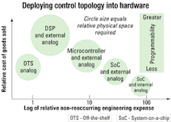
Once a control topology is created, there are several ways it can be deployed in hardware (see Figure 2).Analog-based printed circuit board. An analog control scheme implemented on a printed circuit board (PCB) using off-the-shelf electronics is the easiest and simplest way to develop first prototypes and early production systems. Since the interface to optical devices is analog, developing an all-analog-based system seems the natural thing to do. For single control loops, or even multiple independent loops, implementing control in analog is straightforward and can be done quickly. Specifically, advantages include simple PID-based design, small expense, very fast operation, a short development cycle, and compatibility with low-volume applications. Disadvantages are susceptibility to analog drift and sensitivity to temperature fluctuations. It is practically impossible to do advanced control or implement software programmability in all-analog systems.
Digital-based PCB. The single-biggest attraction of any digital system is programmability. In the case of optical components, it is somewhat of a natural fit, given the advanced control schemes typically required to implement a functional device. Some additional digital advantages for standalone all-optical systems are the ability to combine the control function with the information function.
Applications like optical add/drop multiplexers (OADMs) need to be dynamically reconfigured to support rapid provisioning of MAN systems. The commands for the reconfiguration are directed remotely over the network, and the status and real-time information about the OADM are provided to the central station from an embedded Web server. The digital electronics in this case are multifunctional, effectively combining the control with the device and network management function. These additional software features make installation, service, and support more manageable for customers.
There are disadvantages, however. Digital systems are more expensive to develop than all-analog alternatives and require good firmware engineers. Digital sample-rate preplanning is critical for good performance. Digital approaches also demand more board space.
Custom FPGA with external current loops. Once optical-component suppliers transition from prototype to early production systems to full production, the goal is to reduce the product cost and reduce the size. Implementing an FPGA-based design is a perfect fit for these medium-volume applications.
Tremendous functionality can be obtained from FPGA systems. The approach has the inherent advantages of creating a software-controlled digital system—with the added bonus of being able to appropriately tune the system for high-speed performance—similar to the pure analog system.
Several applications are ideally suited to the parallel processing characteristics of the FPGA. An added bonus is that a development based on a FPGA has software and hardware that are truly system-on-a-chip (SoC)-ready—the ultimate goal once volumes grow. Depending on the vendor and approach used, a very cost-effective development approach can be realized using a combination of FPGAs and external current loops.
Therefore, the advantages of an FPGA-based approach include support of custom control, the provision of a path to a single-chip solution, the ability to be integrated with third-party intellectual property, protection of proprietary control methodology, and the ease with which features can be added. Disadvantages include an expensive development process, the necessity of register transfer level (RTL) programming engineers, the fact that digital sample-rate preplanning is critical, and the requirement for a library and access to RTL blocks.
SoC-based custom IC solutions. Once a supplier's volume approaches 50,000 units per year, the next step in cost and performance improvements is linked to the ability to convert the electronics into a single chip. Once here, there are many tradeoffs and implementation issues that require time to plan and implement. At the heart of the issue is the concept of design reuse—the ability to use intellectual property from multiple suppliers and arrange it in a meaningful way to cost-effectively solve a problem.
The case for hard intellectual property such as RISC and DSP cores is more clear-cut and offers several advantages. Cores can be reused without modification and sometimes offer efficient simulation models. But it is essential that they be supplied with sufficient design views for timing, simulation, and physical-layout tools. It is also widely accepted that starting software development and integration after the receipt of silicon prototypes is a luxury. This approach i ncreases time-to-market and is foolhardy because any fundamental software/hardware integration problem will be caught late in the design cycle and cause even greater delay. For these reasons, a hardware and software co-development approach is desirable. It not only reduces project time scales, but also validates the system architecture, particularly real time software behavior.
Therefore, SoC approaches support advanced control and software programmability. SoC provides the smallest overall size and lowest overall product cost, especially in high-volume applications. Control methodologies can be protected, and SoCs can be very fast. On the other hand, SoCs are the most expensive approach to develop. They require very stable optical design, and digital sample-rate preplanning is critical.
An all-optical crossconnect (OXC) that performs long-haul provisioning-based switching of entire fibers is already quite complex. In this scenario, the OXC is switching a path only and is payload-agnostic—totally unaware of the meaning of the light frames that travel through it. As we move forward, switching times become more critical, switching stability and dynamic response are stringent, and the need for robust closed loop control of optical components becomes an absolute requirement instead of an option.
The development of cost-effective, efficient control electronics promises to increase in importance as optical subsystems and components become more advanced and complex.
John D. Brennan is director of product marketing at Cadence Design Systems Corp. (San Jose, CA). He can be reached via the company's Website, www.cadence.com.


