Design, optimization of planar lightwave circuits using CAD tools
Flexible design interface and complete simulation capabilities are keys in practical design processes.
MATTHEW FRANK, DANIEL HERRMANN, and ZHENGYU HUANG, RSoft Design Group
Driven by the pervasive influence of the Internet and other bandwidth-demanding applications, the telecommunications industry is striving to deliver greater information-carrying capacity. DWDM is one of the few technologies with the potential to deliver the required bandwidth. Even in today's economic environment, market forces are driving the industry to produce systems that combine greater single-channel bandwidth and increased channel capacity.
Key elements in this effort are planar lightwave circuits (PLCs), an attractive concept because of their small size and potential for integration of multiple devices. With recent developments in manufacturing technologies, PLCs are beginning to move out of the research lab and into mainstream applications. The time-sensitive nature of a highly competitive market combined with the previously mentioned market forces make sophisticated computer-aided design (CAD) and numerical simulation tools a critical element to reduce the time from concept to design to production.
We'll examine the application of CAD tools to design and optimize a practical arrayed-waveguide grating (AWG) system. This procedure will mainly use the Beam Propagation Method (BPM); the Finite Difference Time Domain (FDTD) technique will be employed as well.1 The first stage of the design will consist of optimizing the coupling efficiency from a fiber into a PLC. In the next stage, a mode converter will be designed to optimally convert the mode from one PLC into the fundamental mode used for the AWG. The third part of the design process will include the setup of the AWG layout and simulation of the spectral response. And finally, we'll look at individual AWG issues such as flattening the output spectrum, speeding up the simulations, and including bending losses.
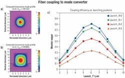
Stage 1Fiber is usually used to connect PLCs to other discrete components. This design raises the issue of reducing the coupling and mode converting loss from a fiber mode to that of the waveguide as well as the return loss to the input fiber. That is especially important for PLCs based on III-V and silicon materials.First, the coupling loss from the fiber to the coupler is calculated. The fundamental mode for both the typical singlemode fiber (see Figure 1a) and the input end of the mode converter (see Figure 1b) were calculated using a BPM-based mode-solver. Then the launching position of the fiber was varied in a CAD tool to optimize the coupling between these two modes.
Results on coupling efficiency from a three-dimensional BPM simulation are shown in Figure 1c. At the optimized launch position, the coupling efficiency can reach about 81% for this particular design. Note that the alignment sensitivity and the coupling efficiency dependence on the launch angle can be obtained from these results.
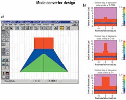
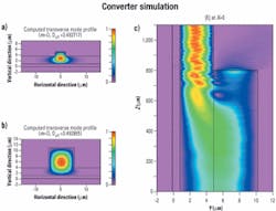
Stage 2Frequently, it is necessary to convert the fiber mode down to the single mode of a PLC. Here, the design process of a silicon waveguide-based mode converter is presented (see Figure 2).2 A mode converter is designed to enable an adiabatic transition between two optical modes. The field will be incident on the converter from a fiber, propagated through the coupler, then output in the fundamental mode of the small rib waveguide. The total percentage of the power coupled from the fiber to the fundamental mode of the smaller rib waveguide will be calculated.Several design considerations can be undertaken to increase the conversion efficiency. Using two tapered waveguides, the overall length of the device can be reduced. Length of the tapers and the relative heights of the layers are also optimized to ensure an adiabatic transition. With a set of optimized taper design parameters, the conversion efficiency can be 94%.
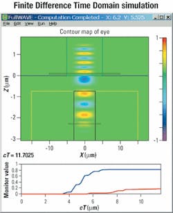
Those simulations are sufficient for coupling efficiency. But if return loss and a more accurate coupling coefficient are desired, other computational methods are necessary due to certain limitations in the algorithm of basic BPM.One method is to use two-dimensional bidirectional BPM. This technique is very fast, but may neglect some three-dimensional (3-D) effects. The other approach is to use a totally different algorithm: the FDTD method, which is a direct solution to Maxwell's equations and accounts for a full array of effects, including reflection for both two- and three-dimensional simulations. The only drawback to this approach is that the FDTD method typically uses much more memory and is more time-consuming than the BPM method. For this type of interface-coupling problem, the FDTD method is still feasible even in a 3-D simulation. Figure 4 demonstrates an FDTD simulation of this system.
Stage 3
After the fiber to the end of the mode converter has been designed and optimized, the AWG design can be undertaken. An NxN AWG comprises N input/output waveguides and two identical star couplers connected by an array of waveguides.3 In operation, the beam propagates through an input waveguide and becomes divergent in the input star coupler. There, the beam is coupled into the waveguide array and propagates through the individual arrayed waveguides into an output star coupler. The optical path length difference between adjacent arrayed waveguides is designed to be a constant. Thus, after propagating through the output star coupler, this beam will be focused at a wavelength-dependent position and coupled into different output waveguides.
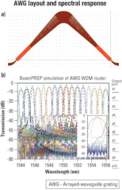
A superior method breaks down the problem into sections that can be simulated separately and combined afterward via a matrix-like approach. The input/output coupler section and waveguide sections are simulated via standard BPM, and the waveguide array is represented simply by a laterally varying phase, derived from the array geometry. The BPM simulation stops at the end of the input star coupler, the phase of the wavefront is calculated and modified based on the characteristics of the array, then the BPM simulation resumes at the beginning of the output star coupler. This process is repeated at each wavelength until the full spectrum is produced. A 16x16 AWG (see Figure 5a) is will be used as an example illustrating the related design and simulation issues.
Stage 4
For a typical AWG design, the transmission spectrum usually has a Gaussian shape with a relatively narrow passband. That leads to a strict requirement on the laser-diode output wavelength and the temperature control of the device. In addition, these (de)mutiplexers are often cascaded in a network, and the combined passband is much narrower than each of the AWG filters separately. Thus, a flattened passband response is desirable.
One effective technique is to use a parabolic taper at the input waveguide side of the first star coupler.3 In a CAD tool, such a taper can be input using an appropriate formula. The taper can be simulated and optimized using the BPM technique until a desired output intensity profile is obtained. Next, by combining this taper design in a 16x16, 100-GHz-spaced AWG, a flattened spectral response is obtained (see Figure 5b). For both designs, the crosstalk level is below 32 dB. The flattened design has a 1-dB bandwidth of about 50 GHz, while the Gaussian spectrum's 1-dB bandwidth is only about 10 GHz. The tradeoff here is that this design has extra insertion loss and a higher adjacent-channel crosstalk level.
The BPM technique used so far is based on a finite difference method (FD-BPM) and is very efficient in simulating this type of PLC. But for an AWG with many channels, the star couplers became very long and a large number of wavelengths need to be simulated. The scheme described above to obtain the spectral response becomes very time-consuming. For instance, it could take tens of hours even on a 1-GHz PC.One effective solution is to break down the simulation scheme further and optimize the simulation parameters and method locally. In the simulation of the device, the wide region in the middle of the star coupler can be accurately simulated by another type of BPM method based on fast Fourier transforms (FFT-BPM). This method yields a very good agreement for both the passband and crosstalk level. Depending on the length of the uniform region versus the rest of the star coupler, which is still simulated using FD-BPM, the simulation time can be shortened by a factor of seven to 10 for this example.
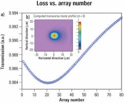
For purposes of the matrix approach used to simulate AWGs, the waveguide array is approximated to first-order accuracy by a laterally varying phase for each wavelength scanned. However, the arrayed-waveguide region can also be simulated separately using BPM. When that is done, information on bending loss, coupling loss, and other effects can be extracted from the BPM simulations and added to the phased-array section in the overall simulation. For instance, the eigenmode of a bend waveguide can be simulated using a BPM-based mode-solver. From the imaginary part of the mode index, the propagation loss can be determined (see the Figure 6 inset).
In the 16x16 AWG example, the bending loss to each arrayed waveguide is calculated according to the geometry, as shown in Figure 6. This information is then added to the entire AWG simulation and a more realistic simulation is obtained. In a similar way, other fabrication-related factors could be simulated separately and incorporated in the overall spectrum simulation.
BPM-based software design tools can be used to simulate both small-scale PLCs, such as a mode converter, and large-scale PLCs, such as an AWG. This kind of design tool offers an integrated design and simulation environment, employs various simulation techniques to provide efficient and accurate design results for a wide array of needs, and provides the capability to simulate both single devices and complex circuits. When used in conjunction with an FDTD-based software package, designers can calculate an even broader group of structures and effects.
Photonics CAD software packages provide optical engineers with a powerful design tool that is easily applicable to a broad range of applications.
Matthew Frank is senior application engineer, Daniel Herrmann is application engineer, and Zhengyu Huang is technical manager at RSoft Design Group (Ossining, NY).
References
- R. Scarmozzio, et al., "Numerical Techniques for Modeling Guided-Wave Photonic Devices," IEEE Journal of Selected Topics in Quantum Electronics, Vol. 6., No. 1, January/February 2000, pp. 150-162.
- D. Gahan, "Integration Technology Advances with an All-Silicon Platform," Lightwave, August 2000.
- K. Okamoto, Fundamentals of Optical Waveguides, Academic Press, San Diego, 2000.
