APDs present biasing, measurement challenges
By Matthew Pilotte
The ever-increasing requirements of today’s optical-network systems require a sensitive device to accurately receive the data and measure optical power. As data rates grow to 10 Gbits/sec and beyond, more and more systems will transition from PIN-type photodiodes to the high-speed capabilities available in avalanche photodiodes (APDs).But for proper operation, the bias applied to the APD must be controlled to maintain a constant avalanche multiplication factor; nonlinear variations of this factor require correction. Ensuring that the bias source is low noise is also critical. Several methods exist for solving this problem.
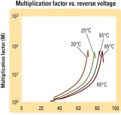
APDs differ from PIN photodiodes in that APDs can provide gain, meaning that the ratio of incoming photons to outgoing electrons is not necessarily 1:1. This ratio, or avalanche multiplication factor (M), is controlled by the reverse bias across the APD. The nonlinear variation of M over temperature and bias control voltage requires correction to accurately use the APD for received signal indication.The large bias voltages required to produce this avalanche effect result in the diode being very sensitive to temperature. Many APD manufacturers provide a temperature coefficient over a specified range (hundreds of mV/°C) or in some cases a plot as shown in Figure 1. Using a temperature sensor coupled to the APD to provide a measure of operating temperature, the reverse bias can be correctly adjusted to maintain stable performance and the desired responsivity. Increasing the bias will improve sensitivity and reduce bit error in the receiver when the incident power is very low; reducing the bias will protect the APD from damage in high-temperature conditions or when the receive power is very large.
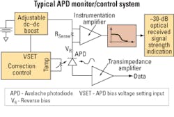
A typical APD monitoring control loop is depicted in Figure 2. The reverse bias applied to the APD must be controlled to maintain a constant M and protect the diode from potential damage due to over-current or over-temperature conditions. Received signal strength indication (RSSI) is provided by using an instrumentation amplifier (in-amp) capable of withstanding the high bias voltages required for the APD.The large components required to implement such filtering can significantly increase the response time of the overall biasing control loop. Response time plays an important role in APD bias control designs because of the high cost of the APD itself. System designers not only want to minimize bit error to maintain the integrity of the received data stream, but they want to be able to quickly decrease the bias to the diode if the ambient temperature becomes too high or the APD begins to draw excessive amounts of current.
Selection of the in-amp is another critical component to the biasing solution shown in Figure 2. An amplifier with high common-mode rejection ratio is necessary to ensure high sensitivity and accurate current measurement across the differential input nodes. The linear nature of the in-amp also limits the amount of measurement range possible to ~30 dB. Switching noise produced by the voltage converter can also cause inaccuracies in the RSSI signal output from the in-amp.
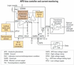
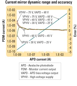
Figure 3 illustrates a modified monitoring control loop. By using the onboard current mirror, a replica of the APD bias current can be directly fed into any current measurement device. Figure 3 shows this monitor current (IPDM) being measured by a translinear logarithmic amplifier. Using a log amp enables wide dynamic range measurements of the incident optical power, up to 70 dB with 0.1-dB accuracy, without the dynamic range limitation that would result in an in-amp current-sensing solution. A plot of the dynamic range and accuracy of the current mirror using this new approach is shown in Figure 4.
The ability to fine-tune the applied APD potential by using a low-voltage ground-referenced input signal to the APD bias voltage setting input (VSET) pin enables the use of a lower-cost fixed dc-dc boost converter. The fixed dc-dc converter is more easily filtered to remove the inherent ripple current associated with any switching-based voltage converter. Because the bias to the APD is controlled by the bias controller/current monitor and not the voltage converter (as in Figure 2), the response time of the control loop is no longer limited by filtering on the converter or in-amp outputs. That permits a more compact and lower-cost design of the high-voltage supply circuitry.
The high cost of APDs leads to the need for integrated protection circuitry to prevent damage to the diode. The FALT pin is an open collector logic output (active low) that provides the designer with an indication of a potentially hazardous operating condition that could harm the APD. If the current at APD bias node (VAPD) begins to draw >18 mA, the FALT pin will assert and the current mirror will shut down, reducing the current to the diode as well as the bias voltage. Thermal protection is also provided to prevent damage to the bias controller/current monitor. When the die temperature exceeds 140°C, the current mirror will shut down, allowing VAPD to drop, and FALT will assert. The device will remain in this protected mode until the die temperature falls ~20°C.
The high speed of next generation optical networks will require APDs to achieve accurate transmission of data and low bit-error rates. Accurate control of the voltage bias across the APD is critical to the success of these systems. The bias controller/current monitor enables linear control of these bias levels and simultaneous monitoring of the photodiode current to maintain the appropriate M for the temperature and optical-signal-level conditions, without the need for additional filtering requirements typically caused by voltage converters.Matthew Pilotte is an applications engineer in Analog Devices’ Advanced Linear Products Division (Wilmington, MA).


