Avalanche photodiodes poised for 10-Gbit/sec applications
The internal gain of an avalanche photodiode makes it a key enabler in the manufacturing of high-sensitivity optical receivers.
The pervasive need for greater cross-sectional bandwidth in fiber-optic network links is cited so often in industry literature, it is with some reluctance that this author invokes this pronouncement yet again. Nevertheless, forecasts of an exponential increase in data-transmission volume over the next decade seem unassailable, and the deployment of an infrastructure capable of handling all this information has been a very real driver for vast improvements in system performance.
Wherever possible, to avoid the expensive alternative of installing more optical fiber, system designers are leveraging technological advances of two types: higher bit transmission rates (time-division multiplexing--TDM) and a greater number of wavelength channels (wavelength-division multiplexing--WDM). The challenge of developing component-level devices with adequately enhanced performance must be met by component manufacturers, and there has been substantial progress in numerous areas. One example is the development of high-sensitivity optical receivers for performing optical-to-electrical signal conversion at data rates of at least 10 Gbits/sec.
The canonical fiber-optic receiver for long-wavelength signals (1310 or 1550 nm) contains an indium gallium arsenide (InGaAs)/indium phosphide (InP) photodiode, a transimpedance amplifier (TIA), post-amplification, clock- and data-recovery circuitry, and electrical demultiplexing of the high-frequency bit stream. The sensitivity of a receiver (the lowest signal power detected with an acceptably low bit-error rate) depends critically on the front-end elements. In particular, there are two common choices for the photodiode element: the standard PIN diode structure, and the avalanche photodiode (APD). Although the APD requires higher operating voltages, which must be compensated for temperature shifts, its internal gain provides a significant enhancement in receiver sensitivity and can be a key enabler in the manufacturing of high-sensitivity optical receivers for 10-Gbit/sec applications.
The photocurrent of a PIN diode is intrinsically quantum-limited. At best, each input photon results in only a single electron-hole pair to contribute to the total photocurrent. On the other hand, an APD exhibits internal gain through avalanche multiplication. In the presence of sufficiently high electric field intensity, an initial photon-induced carrier can seed an avalanche process in which carriers obtain enough energy from the electric field to generate additional carrier pairs through impact ionization. By such an effect, a single photon can give rise to tens or even hundreds of carriers that contribute to the resulting photocurrent.
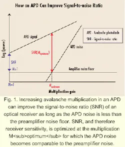
The avalanche multiplication process is inherently noisy because it is stochastic. Under a specific bias condition, the average multiplication gain M is generally the most likely number of carrier pairs created by a given photon. There is, however, also a significant probability that any given photon will give rise to M-1 pairs, M+1 pairs, or some other value within a distribution around M. This "excess noise" contribution (which is gain-dependent) can make the APD much noisier than a PIN diode in an absolute sense. But the comparative usefulness of these devices must be considered in the context of the entire receiver.Figure 1 illustrates how an APD can increase receiver signal-to-noise ratio (SNR), which is directly related to sensitivity. A fundamental noise limitation of an optical receiver is the noise floor of the amplifier that follows the photodiode. The signal and noise of an APD with unity gain (M=1) are nominally identical to those of a PIN diode; the SNR under this condition is illustrated along the ordinate of Figure 1. An increase in the APD signal can be achieved by increasing the gain (along the abscissa) which leads to a direct increase in the receiver SNR as long as the APD noise remains less than the amplifier noise floor. The SNR is maximized at an optimum value of the APD gain for which the APD noise is approximately equal to the amplifier noise. Note that this is true even though the APD noise may increase faster with gain than the APD signal does.
For low-frequency applications, amplifiers can be designed with extremely low noise. Therefore, in the context of lower-frequency digital transmission, the use of an APD provides no significant benefit. At higher bit rates such as 2.5 and 10 Gbits/sec, however, the sensitivity enhancement of an APD-based receiver can be considerable relative to a comparably designed PIN-based receiver.
For InGaAs/InP APDs appropriate to long-wavelength telecommunications signals, APD receivers designed for 2.5-Gbit/sec signals typically provide at least 7-dB improvement relative to PIN receivers. For data rates of 10 Gbits/sec, this improvement is currently about 5 to 6 dB.
On a simplistic level, higher sensitivity in an optical receiver has obvious merit. One measure can be crudely extracted from the cost of optical amplification, which is roughly $1000 per decibel. If an APD receiver at 2.5 Gbits/sec can add 7 dB to a designer's power budget for a few hundred dollars more than a PIN receiver, then the economic advantage of an APD solution is self-evident.
The APD receiver also offers greater flexibility through its wider dynamic range. The complexities of system design at 10 Gbits/sec, however, introduce additional considerations. For
example, in a situation where fiber-induced dispersion poses a greater constraint on signal-propagation length than fiber-induced signal attenuation, the higher sensitivity of an APD receiver might seem to offer little advantage. But additional margin in the power budget can provide tolerance for the losses associated with components such as dispersion compensation modules, which help to alleviate the fundamental dispersion constraints.
Another context in which the benefit of APD receivers might seem questionable is that of multiple wavelength channels present on a single fiber. If all channels can be simultaneously optically amplified before being split off to PIN receivers, then the optical amplification cost per decibel can be lowered by spreading it among all the wavelength channels. APD receivers will remain relevant in this situation as long as the design of the APD chip itself enables future costs that do not compare too unfavorably with those of PIN diodes.
Furthermore, this realization of point-to-point multichannel transport may have more limited scope in the near future. There is a much greater desire for flexible networks in which wavelength channels serve as the coarse-grained units to be independently added, dropped, and otherwise manipulated. In this scenario, the additional sensitivity of APD-based receivers will provide an inexpensive power budget margin for the many network branches that will inevitably be introduced to handle individual wavelengths.
Taking for granted the utility of the APD-based receiver, the next challenge is to design a high-performance APD for use at high bit rates that is reliable and manufacturable. The desire to detect wavelengths in the 1300- to 1600-nm range dictates the use of an In0.53Ga0.47As absorption layer-grown lattice matched to an InP substrate, as in standard telecommunications PIN diodes. The need to achieve avalanche multiplication requires the presence of sufficiently high electric fields, but the narrow bandgap InGaAs (Eg ~ 0.75 eV) suffers from intolerably large tunneling leakage currents at electric fields lower than those required to exhibit significant avalanche multiplication in this material.The ubiquitous solution to this problem has been the adoption of the separate absorption and multiplication (SAM) APD structure in which the absorption and multiplication functions are relegated to different layers of the device. A field-control layer of moderately doped InP is designed to maintain low electric field in the InGaAs absorption layer while supporting high field in an InP multiplication layer (see Fig. 2). The wider bandgap InP (Eg ~ 1.35 eV) exhibits avalanche multiplication without tunneling and is transparent to wavelengths longer than 0.95 micron.
The SAM-APD structure has been adopted in all commercially available APDs for long-wavelength telecommunications applications, but beyond this rudimentary concept, design details vary widely. Unlike the standard PIN diode (a device with sufficient maturity that virtually all the commercial offerings are quite similar in design), the InGaAs/InP APD exists in many variations.
Regardless of bit rate, perhaps the most critical APD design issue is maintaining gain uniformity across the active area of the device. The tendency for enhancement of electric fields at the edge of the active area is a basic property of the physics of finite-size planar positive-negative (p-n) junctions. These enhanced edge fields lead to larger gain at the device edges and premature "edge breakdown," which has harmful effects on device performance. The key to alleviating edge breakdown is to reduce the electric field intensity at the device edges, and device designers have come up with numerous approaches to solving this problem.
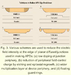
Techniques for controlling edge breakdown in planar junctions can be grouped into three general approaches (see Fig. 3):
- Low doping density at junction edges (conventional guard rings)
- Control of the total charge profile in the field-control layer
- Control of the junction profile.
In the first approach, edge fields are reduced by using a lower doping density in the device periphery than in the device center (see Fig. 3a). This has been accomplished using ion implantation or low-temperature diffusion of an appropriate dopant that is different from the dopant used to create the central region of the junction. The second technique requires two epitaxial growth steps: epitaxy is carried out up to the field-control layer where a mesa etch is performed, and then a subsequent epitaxial regrowth completes the structure (see Fig. 3b). In the third approach, a junction of constant doping density is shaped to create a wider multiplication region with consequently lower electric fields in the peripheral region of the device (see Fig. 3c). A related concept is the use of "floating" guard rings, which have the same doping as the central region but are electrically isolated from it and tend to lower the surface electric fields when the junction is biased (see Fig. 3d).
Another APD design, based on the third concept described above, makes use of both a shaped junction profile, created using two diffusions and floating guard rings. An attractive aspect of this approach is that the device can be fabricated using a simple, technologically mature diffusion process, widely used in making standard PIN diodes. This consistency in fabrication technique provides these APDs with the same level of process control present in PIN-diode manufacturing along with comparably high reliability.
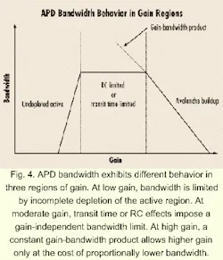
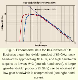
Having mastered a technique for controlling edge breakdown, a remaining obstacle to producing a 10-Gbit/sec APD is attaining sufficiently high bandwidth. There are three distinct gain regions in which different phenomena pose limiting bandwidth factors (see Fig. 4). In the low-gain region, the internal electric field does not extend across the absorption layer, and high bandwidth cannot be achieved because photoexcited carriers will experience only a slow, diffusive motion. At moderate gains, carriers are swept by a finite electric field across the entire device (see Fig. 2), and the bandwidth limitation in this region is either the carrier transit time or the resistance capacitance (RC) time constant due to the parasitic resistance and capacitance of the device.For high-gain operation, the time for the avalanche process to occur in the multiplication region becomes the bandwidth-limiting factor; the larger the gain, the longer the avalanche process takes. In this region, gain and bandwidth are inversely related and characterized by a constant gain-bandwidth (G-BW) product. A substantial amount of research on multiple quantum wells (also referred to as superlattice structures) has been focused on increasing the G-BW product by bandgap engineering. Larger G-BW products can also be obtained in simple bulk materials (e.g., InP) by using thinner multiplication layers.
For use in 10-Gbit/sec receivers, APDs should achieve at least 7 to 8 GHz of bandwidth over the desired range of operating gain. Maximum sensitivity is typically found for multiplication gains of M~10, which dictates that G-BW products of 80 GHz or more are desired. The epitaxial layer thickness and device area must be designed so that the transit time and RC time constant do not limit the bandwidth to less than 8 GHz.It is also important to achieve high bandwidth at low gain: Larger optical powers that overload the preamplifier at high APD gain can be accommodated if the APD can be operated at low gain while still maintaining sufficient bandwidth. Generally, there is a tradeoff between high bandwidth at low gain and at high gain (see Fig. 5). If the APD is not the bandwidth-limiting element in the receiver when the gain is optimized for sensitivity (i.e., M~10), compromising high-gain bandwidth to obtain high bandwidth at lower gain will enhance the receiver's dynamic range. Receivers based on these APDs can achieve -26-dBm sensitivity (at a 10-10 bit-error rate) using gallium arsenide (GaAs) pseudomorphic high electron mobility transistor (p-HEMT) TIAs. This performance represents a 5- to 6-dB sensitivity enhancement relative to comparably designed PIN-based receivers.
Through the use of good design strategies, which can be implemented using established fabrication technologies, it has been possible to develop reliable, manufacturable APDs for use in 10-Gbit/sec optical receivers. Although these devices are still considerably more difficult to make than 2.5-Gbit/sec APDs, the fact that the same design approach was feasible at both bit rates has contributed substantially to the success of 10-Gbit/sec APDs. Yield and reproducibility will continue to improve as the epitaxial growth of this material progresses. Unlike the migration from 2.5- to 10-Gbit/sec APDs, however, it is almost certain that new approaches will be necessary to achieve the next jump in bit rate to 40-Gbit/sec performance.
Designing APDs for the next generation of optical receivers at 40 Gbits/sec will require the surmounting of at least two major challenges: obtaining G-BW products of several hundred gigahertz and reducing transit times to permit bandwidths approaching 40 GHz. To obtain extremely high G-BW products, avalanche regions will need to be extremely thin (less than 0.1 micron), and structures with improved avalanche properties may be beneficial. As a bulk material avalanche region, silicon (Si) has avalanche properties superior to those of InP. It cannot be directly grown on InP-based structures since the atomic lattice constants of these two materials are not well-matched, but experiments involving wafer fusion bonding have shown the possibility of combining an Si multiplication region with an InGaAs absorption region. Among lattice-matched compounds, indium aluminum arsenide (InAlAs) holds promise for improving on the avalanche properties of InP. Well-designed superlattice structures may also aid in reaching much higher G-BW products.
The second challenge to 40-Gbit/sec performance--transit time limitations--will dictate the use of much thinner absorption layers for which the transit time varies linearly with layer thickness. The consequent increase in speed comes with reduced quantum efficiency assuming that the optical signal experiences a single pass through a conventional surface-normal illuminated structure. As with PIN photodiodes at microwave frequencies, this bandwidth-quantum efficiency tradeoff can be circumvented using different device geometries.
It's possible to obtain higher quantum efficiency with an edge-illuminated waveguide structure in which the core of the waveguide is a very thin absorption layer. In this case, the absorbed optical power is spread along the length of the waveguide nearly instantaneously (at the speed of light), and the photoexcited carriers can then be collected very quickly across the thin absorption layer in a direction perpendicular to the optical path. A significant challenge in using this structure is the coupling between an optical fiber and the waveguide.
Alternatively, a surface-normal illumination geometry can be maintained by embedding a very thin absorption layer in a resonant cavity composed of epitaxially grown quarter-wave stack mirrors. In such a structure, multiple cavity reflections allow almost all the optical power to be deposited in a thin (and therefore high-bandwidth) absorption layer. A limitation of the resonant cavity approach is that the spectral response is fairly narrow (but not narrow enough to discriminate between dense wavelength-division multiplexing channels) and must be carefully tuned.
Although there are encouraging examples of techniques that may be suitable for designing commercial APDs capable of 40-Gbit/sec performance, considerable work remains to prepare these devices for deployment. For applications at 10 Gbits/sec, however, it is clear that APDs are poised for widespread use.
Mark Itzler is the director of research and development at EPITAXX Inc. (West Trenton, NJ).
