Nano-optics changes the rules for optical components
New subwavelength optical elements promise significant decreases in component size.
Hubert Kostal
NanoOpto Corp.
The speed at which optical networking proliferates is currently constrained by the lack of availability of functionally integrated, cost-effective optical components. Just now entering commercial development are wafer-based, nano-fabrication techniques that allow the creation of a new class of optical components -- Subwavelength Optical Elements (SOEs) -- with physical structures far smaller than the wavelength of light.
The fine-scale surface structures of SOEs interact with light according to novel physical principles, yielding new arrangements of optical processing functions with greater density, more robust performance, and greater levels of integration when compared to many existing technologies. Even more exciting is the promise for the near future. The extremely small dimensions of SOEs allow multi-layer integration, yielding complex optical components "on a chip" with broad application to optical networking and with the potential for fundamentally new approaches to optical systems design.
Optical networking and optical components
Optical networks are uniquely suited to handle the ultra-high traffic demands in core and metro core networks, and the continuing growth of broadband services is driving the requirement for optical networking further into the metro and access networks. In general, the growth of optical networks is paced by aggregate traffic volumes, data-driven applications, broadband services, government regulations, and the cost/performance of optical networking technology.
Focusing on the physical network itself, the economic combination of network architectures and system capabilities determines the feasible boundaries of optical networking. First, optical networking architectures become more efficient with the introduction of wavelength management and services -- using DWDM not only for capacity enhancement but also for the independent management of optical channels with greater granularity. This provides a service-independent routing capability in the optical domain and simplifies the interaction with electrically based switching elements.
Second, optical networking systems are still relatively new. There exists great opportunity for cost reduction through increased integration, improvements in manufacturing and yields, and through the introduction of new technologies. The required improvements in architecture and systems are inherently dependent on the optical component technology.
The current state of optical components is simultaneously invigorating and confusing. There is a vast array of natural materials and optical effects that can be drawn on to create the basic functions required for optical processing -- spanning basic splitting and coupling, polarization management, wavelength management, switching, attenuation, photo detectors, transmitters, receivers, and amplification. The optical component and system designer must exhibit great creativity. However, the lack of a basic design vocabulary limits structured design approaches and complicates higher degrees of functional integration. This inconsistency in optical component technologies leads to increased cost, and implied systems cost; lack of integration; lack of density; and a general lack of methods for high volume, scalable manufacturing.
Nano-optics: A new class of optical components
SOEs provide a set of basic optical building blocks for the construction of optical components and systems. These devices are compact and flexible, and support a high degree of integration. More significantly, SOEs are tailored optical components, whose optical properties can be varied to meet various optical design requirements.
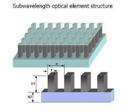
An SOE is an optical chip, in its simplest realization a substrate with a nano-structure on its surface topped with a protective layer (Figure 1). The nano-structure has one or more dimensions far smaller -- on the order of tens of nanometers -- than the wavelength of light used in optical communications. In a free-space application, light is normally incident on the SOE chip. The physical interaction of light with the nanostructure obeys the rigorous application of the physics of diffraction gratings, but the scale of the structure causes changes in the boundary effects, resulting in uniform behavior over a broad wavelength range, wide acceptance angles, and the ability to create multiple optical effects simply by varying dimensions. The materials used can also be selected to determine optical effects and ensure high damage thresholds
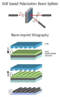
By controlling SOE nano-structure shapes, dimensions, relationships and materials, a broad range of optical functions can be created, including but not limited to polarizers; polarization beam splitters/combiners (Figure 2); waveplates; filters, both fixed and tunable; microlens arrays; photo detectors; and switches. These devices are ideally suited for broad application in optical components, from transmitters to switches to optical signal conditioning.
While the concept of light interacting with a nano-structure has been the object of scientific investigation for at least 20 years, optical devices using these effects have not been generally commercialized to date. This is because there has not been a low-cost, fast, broadly applicable manufacturing process that can be used to create general nano-patterns.
Nano-fabrication utilizing nano-imprint lithography addresses that need. This wafer-scale manufacturing process uses a re-usable mold, on which the negative of the desired nano-structure has been created, to impresses a nano-structure onto a resist layer which is then transferred to the desired material via reactive ion etching (Figure 3). This nano-manufacturing process is highly repeatable, high speed, and automated.
Multiple optical devices (the entire list above has been demonstrated) can be created using the same manufacturing process, switching the molds and making minor adjustments to the materials used. The manufacturing process allows fine-scale control to be exercised over the nano-structure dimensions, allowing the optical performance of discrete SOE devices to be formulated to address specific optical applications.
Several demonstrable optical component and system cost reductions result from the combined application of SOE optical components and nano-imprint lithography-based nano-manufacturing. Initially, optical component and system cost reductions result from the increased density that can be obtained using SOE optical chips, allowing greater density at the board and system level. In many cases they enable simplified device architectures that reduce optical subcomponents count and bill-of-materials cost. The combination of high damage threshold and wide acceptance angle results in ease of integration and assembly. Finally, because SOE components are manufactured on a wafer scale, the per-component cost can be expected to dramatically reduce with increasing volume.
Next steps for SOE optical chips
The initial introduction of SOE optical chips provides discrete optical functions. These SOEs can be integrated heterogeneously or monolithically. Heterogeneous integration takes advantage of the thin-film nature of SOE material. The SOE can be placed directly adjacent to, affixed to, or inserted into other optical components, such as lasers, planar lightwave circuits, and other devices. This readily increases the functional density of existing optical component technologies.
Even greater density can be achieved via monolithic integration. This is principally accomplished by layering SOEs within the nano-manufacturing process. The stacking of optical functionality can be used to create a range of useful devices, simply concatenating functionality that would currently be performed in a sequence of elements. An example of an immediate capability is the integration of a photodetector with a filter, creating an optical chip with the basic function required for optical feedback loops or optical performance monitoring.
The introduction of the initial SOE devices -- polarizer, polarization beam splitter, and polarization beam combiner -- will allow exploration and refinement of new component architectures in applications ranging from transmitters to amplifiers to isolators to optical switches. The introduction of additional SOE optical functional and integration should spark dramatic changes to the shape of optical components over the next few years, with subsequent impact on the economics of optical networking.
Hubert Kostal is vice president, marketing and sales, at NanoOpto Corp. (Somerset, NJ); www.NanoOpto.com. He can be reached at [email protected].
Figure 3 (bottom). Nano-imprint lithography is essentially a three-step process. In Step 1, a mold containing negative of the desired structure is impressed into a combination of resist material, target material, and substrate. In Step 2, the mold is removed, leaving a nano-pattern impression in the resist material. In Step 3, etch techniques are used with the resist material to transfer the pattern to the target layer.


