Nanofabrication tools promise new laser manufacturing methods
The recent advances in nanofabrication provide many new opportunities to develop new devices that are cheaper and better than conventional alternatives. Quantum dot lasers, NanoOpto’s polarizers, splitters, and waveplates are some examples of the products from “nano-engineering” processes. Another nanofabrication technique that shows promise is focused ion beam (FIB) etching, which is a new method of fabricating singlemode semiconductor and surface-emitting lasers.
Most conventional singlemode lasers rely on distributed feedback (DFB) and distributed Bragg reflector (DBR) designs. Both of these designs typically require periodic grating deposition and multiple epitaxial growths on the semiconductor wafer.
Alternative designs based on coupled cavity effects within two-section lasers have also been investigated. However, the stability and performance of such singlemode devices requires careful control over the air gap between the two cavity sections. Devices such as cleaved-coupled-cavity (C3) lasers have been shown to achieve singlemode operation but so far have not been commercially deployed. The difficulties of implementing the C3 lasers include the lack of consistency in the control over the air gap between the two laser cavity sections and the laser stability over aging and environmental conditions.
In 1992, a group of scientists at Bellcore demonstrated the use of FIB etching to develop Fabry-Perot (FP) lasers that could emit their output light from the wafer surface. However, these lasers exhibited rather low output power. Recent advances in FIB technology and the commercial availability of precision dual-beam scanning electron microscope (SEM)/FIB instruments now allows improved control of the process and enables new applications.
The FIB process has already been demonstrated for creating novel nanostructures in many materials, as well as preparation of ultrathin material samples for microscopy, nanoprototyping, nanometrology, circuit trimming, and photomask repair. A gallium (Ga+) ion source is typically used, and the resolution of the FIB can be as small as 5 nm.
The modern FIB is a very flexible processing tool that can be applied to any target material at any arbitrary angle, shape, and size. Simply, the FIB process is similar to a nanomilling machine. This is especially useful for defining laser cavities in materials that are not suitable for cleaving, such as GaN. Unlike many dry-etching methods, FIB etching is a “maskless” process. It is a post-fabrication process that can be applied to prescreened lasers, which reduces product manufacturing costs. The FIB process can be automated and applied on a wafer scale.
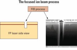
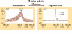
FIB etching into the waveguide can convert low-cost FP lasers to singlemode coupled-cavity lasers. Figure 1 shows the schematic diagram of a FIB-etched FP laser and a SEM picture of the cross-section of the FIB cut. In this demonstration, an InAlGaAs ridge waveguide FP laser emitting at 1,310 nm was FIB etched to create an air gap along the waveguide. The performance of the laser depends on the relative optical length of the two cavities, the gap distance, and the reflectivities of the facets. “Mode hopping” can be suppressed by choosing a long-short cavity design. The FIB process enables the precise control over the spacing between the coupled cavities to the nanometer scale. The FIB etching process also produces very high quality, very smooth mirror surfaces.Currently, singlemode DFB lasers cost 10 to 20 times more than multimode FP lasers. Converting an FP laser into a singlemode laser using the FIB technology substantially reduces singlemode laser costs. The FIB process can be automated and applied on a wafer scale. It is also a post-fabrication process that can be applied to prescreened laser wafers. Therefore, the FIB processing cost per laser should be very low. The availability of low-cost singlemode lasers will open new applications for the fiber-optic industry.
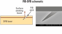
The success of vertical-cavity surface-emitting lasers (VCSELs) at 850 nm has attracted large investments in the development of long-wavelength (1,310 and 1,550 nm) devices. The VCSEL cost is low because the die size is small, and the technology allows wafer-level testing and characterization. However, due to many material constraints, development has been slow and difficult. Therefore, the current deployment of long-wavelength VCSELs is still limited.FIB etching provides an alternative path toward surface-emitting lasers via a 45° cut to an edge-emitting laser. A schematic of the FIB-DFB and the SEM cross-section of the angle FIB etch are shown in Figure 3. A 1,550-nm InGaAsP buried heterostructure DFB laser was used in this experiment. The angle of the FIB etch could be controlled by tilting the mechanical stage and the ion beam focusing parameters.
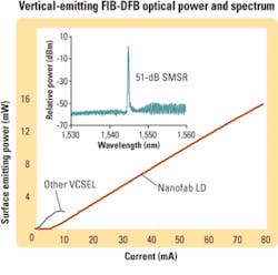
The power versus current curve and spectrum are shown in Figure 4. More than 15 mW of vertical emitting power and singlemode operation with 51-dB SMSR have been demonstrated. By taking advantage of a longer horizontal gain region, the FIB surface-emitting laser power is more than 10× higher than a commercially available long-wavelength VCSEL.
FIB processing can also be applied to FP lasers. In such folded cavity lasers, the top surface of the chip provides the feedback to form the lasing cavity. The FIB-DFB laser does not rely on feedback from the top surface for lasing; therefore, the surface emission angle is not restricted to 90° and can be adjusted by the FIB angle.
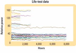
Since a high-energy Ga+ ion beam is used for the etching process, surface defects and Ga ion redeposition are introduced during the FIB process. Defects can cause local optical absorption and heating, which reduce the lifetime of the device. Devices without proper FIB processing and treatment may only survive from a few hours to a few days.Researchers have been studying methods to eliminate such defects by controlling the ion beam parameters and post-FIB “cleaning” processes. Over 200,000 accelerated life-test hours have been performed on FIB lasers created using one such propriety post-cleaning process. Figure 5 shows data from 43 FIB lasers in life tests at 200 mA and 100°C, grouped into four batches and subjected to life tests at different starting times. The earliest batch has been in life test for more than 8,000 hours, and no device degradation has been observed so far.
FIB etching is not the only method to create etched laser facets. Chemically assisted ion beam etching (CAIBE), reactive ion beam etching (RIBE), and anisotropic reactive ion etching (RIE) have also been used to etch laser facets. Each method has its own advantages. Commercial companies such as BinOptics and Xponent Photonics recently reported proprietary etched-facet semiconductor lasers with excellent reliability. The important consideration in choosing an etching method relies on knowing what is needed for etching precision, depth, surface quality, speed, and manufacturability.
The FIB process can be used to fabricate high-speed, short-cavity lasers, since shortening of laser cavities is often used to increase laser modulation speed. Conventional laser cleaving limits the cavity length to approximately 200 µm in production, whereas the FIB process can etch laser facets to any arbitrary cavity length. It can also be applied to any waveguide geometry to create mirrors, beam splitters, gratings, microresonant cavities, and wavelength-selected elements. Multiple FIB elements can be used to create an integrated photonic chip. FIB thereby provides a nanofabrication technology platform for a new class of photonic integration devices.Norman Kwong is the CTO and cofounder of Archcom Technology Inc. (www.archcomtech.com). Axel Scherer is the Bernard A. Neches Professor of electrical engineering, applied physics, and physics at the California Institute of Technology.
*The authors wish to acknowledge DARPA for its support of Caltech’s effort under HR-0011-04-1-0054.
