Intel demos Tofino 2 Ethernet switch with co-packaged optics
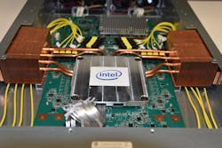
Intel is offering demonstrations of its 12.8-Tbps programmable Tofino 2 Ethernet switch (gained via the Barefoot Networks acquisition) co-packaged with 1.6-Tbps silicon photonics engines. The demonstrations, originally scheduled for OFC 2020, are taking place this week at an Intel facility.
The demonstration, which Intel Director, Strategic Marketing and Business Development Robert Blum called “a path to a product,” leverages a silicon photonic engine with such features as an on-chip laser, detectors, and resonate ring modulator. It accepts 16 electrical I/Os on the host side and supports a total of 16 PAM4-based parallel optical lanes traveling on parallel single-mode fibers, on the panel side. The 16 optical channels are configured as four ports of 400GBase-DR4 interfaces. The switch/optics combination does not require changes to the switch I/O, added Blum and Prem Jonnalagadda, senior director, product management and marketing at the Barefoot Networks Division of Intel. However, the Tofino 2 optimized for co-packaged optics ships in a multi-die package that makes it easier to upgrade the SerDes for lower power or higher throughput, said Intel via a press release.
While Intel plans to offer complete switch/co-packaged optics products, the co-packaged optics approach is applicable to switches designed by companies other than Intel, said Blum and Jonnalagadda, as long as the switch chip has the necessary onboard short-reach SerDes I/O capabilities. The company is in the process of contacting potential partners to ensure applicability to such initiatives as that Facebook and Microsoft have launched (see “Microsoft, Facebook form Co-Packaged Optics Collaboration”).
The demonstration sees the switch/optics co-packaging implemented in an air-cooled 2RU Ethernet switch. The optical technology that composes the demonstration is capable of scaling to 3.2 Tbps or more, says Blum. He predicted that co-packaged approaches will begin to ramp significantly once switches reach 51.2 Tbps with 100-Gbps I/O.
For related articles, visit the Optical Technologies Topic Center.
For more information on optical components and suppliers, visit the Lightwave Buyer’s Guide.
To stay abreast of optical communications technology, subscribe to Lightwave’s Enabling Technologies Newsletter.
About the Author

Stephen Hardy
Editorial Director and Associate Publisher, Lightwave
Stephen Hardy is editorial director and associate publisher of Lightwave and Broadband Technology Report, part of the Lighting & Technology Group at Endeavor Business Media. Stephen is responsible for establishing and executing editorial strategy across the both brands’ websites, email newsletters, events, and other information products. He has covered the fiber-optics space for more than 20 years, and communications and technology for more than 35 years. During his tenure, Lightwave has received awards from Folio: and the American Society of Business Press Editors (ASBPE) for editorial excellence. Prior to joining Lightwave in 1997, Stephen worked for Telecommunications magazine and the Journal of Electronic Defense.
Stephen has moderated panels at numerous events, including the Optica Executive Forum, ECOC, and SCTE Cable-Tec Expo. He also is program director for the Lightwave Innovation Reviews and the Diamond Technology Reviews.
He has written numerous articles in all aspects of optical communications and fiber-optic networks, including fiber to the home (FTTH), PON, optical components, DWDM, fiber cables, packet optical transport, optical transceivers, lasers, fiber optic testing, and more.
You can connect with Stephen on LinkedIn as well as Twitter.
