Nano-optics support multiple approaches of integration -- monolithic and hybrid -- into optical components, allowing for a wide diversity of applications.
Hubert Kostal
NanoOpto
While there are many clever ways to design and build networks and systems, the fundamental breakthrough required to meet dramatically reduced cost points is the introduction of viable photonic ICs. Although there are physical differences between photons and electrons that make exact comparison an area for debate, the evolution of electronic ICs does provide a guide for the direction required for photonics. Paralleling the evolution of electrical circuits, the development of photonic ICs promises to increase functionality and density and significantly reduce costs when compared to optical components assembled from discrete devices. The result will open more general systems and service applications for optical networks.
There are three core criteria any integrating technology must meet:
1. The technology must be capable of creating a broad range of optical functions out of a single fabric or process.
2. The means must exist for it to be readily manufactured at low cost in high volume.
3. The capability must exist to aggregate individual optical functions into more complex arrangements within the technology and with other optical technologies.
Nano-optic devices and manufacturing
Standalone nano-optic devices typically consist of nano-scale structures, <1 mm thick, with individual feature sizes controlled to dimensions of <10 nm, on an optically transparent substrate. As incident light passes through the nano-structures, a portion of the light is transmitted and a portion is reflected.
Changing the arrangement and material of the nano-structures modifies the resulting optical function as well as the degree to which it is applied to the transmitted and reflected components of light. Demonstrated functionality created from nano-structures includes polarizers, polarization-beam splitters and combiners, waveplates, fixed and tunable filters, microlenses, antireflection coatings, and photodetectors.
In simpler applications, including polarization, phase management, and filtering, the nano-structure is a diffraction grating with critical dimensions an order of magnitude smaller that the wavelength of incident light -- on the order of a few hundreds to tens of nanometers. Since modifying the arrangement and materials will tailor their optical performance, nano-optic structures can be considered a core set of photonic building blocks, addressing the first challenge.
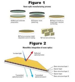
Nano-optic devices are manufactured on a wafer scale in a semiconductor-like manufacturing process that results in optical chips in sizes from 1x1 mm and 0.2 mm thick up to tens of millimeters to a side and 1 mm thick (see Figure 1). The first step in realizing a nano-optic device is to design the nano-pattern that yields the desired optical properties. That can be done through a combination of simulation and prototyping. Once a design is finalized, a mold is prepared that has the complement of the desired pattern inscribed in it. Various lithography techniques, including holographic lithography and e-beam lithography, can be used to create the mold.
In production, the mold is contacted with a prepared substrate -- consisting of a pliable polymer resist layer, a layer of the target material for the nano-structure, and an optically transparent substrate -- and the nano-structure pattern is transferred to a pliable polymer resist layer. This mode of pattern transfer is used to avoid the errors that result due to reflection, diffraction, and scattering effects associated with using higher-energy lithography methods at such fine dimensions. Since the manufacturing method is the same for any nano-optic produced -- fundamentally only the mold and the settings for each processing step are varied -- the same manufacturing line is used for the full range of devices. By combining well-understood nano-structure pattern transfer methods and semiconductor processing methods, nano-optics meet the second challenge.
Monolithic integration
Because of their physics and the manufacturing process used to create them, nano-optic structures can be combined in multiple ways, both with themselves (monolithic integration) and with other materials and processes (hybrid integration) to yield integrated photonic devices.
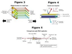
When processing a single beam of light (or multiple beams identically), the straightforward approach to monolithic integration is to sequence optical functions. In the nano-optic paradigm, that is achieved by stacking nano-structures on a single substrate using multiple passes through the manufacturing process to create a summation of optical functions. By appropriately choosing the optical functions and their sequence, useful optical functions can be created.
A simple application is to combine waveplate and polarizer layers to create a circular polarizer. More complex configurations are possible, incorporating spacer layers to achieve walkoff in multiple beam components and reflective layers or waveguide layers to redirect both reflected and transmitted beams (see Figure 2). The benefit of layered nano-optic devices is the ability to combine adjacent optical functions into much smaller, denser devices that can either encompass the full function of an optical component or allow the optical component to be significantly reduced in size.
A second type of monolithic integration requires the processing of multiple parallel beams of light discretely in a single device. That's accomplished by using an array of differing optical functions on a single horizontal layer. A master mold consisting of an array of nano-optic functions is created by using multiple masking and lithography steps. Since this complex sequence is captured in the mold and does not need to be repeated in regular manufacture, it lends itself to ready replication. That is distinctly different from technologies whereby optical materials are created from thin films, crystals, or self-assembling structures, since those methods produce uniform layers.
In a broad range of optical components, the incident optical beams are split into two beams, which are differentially processed, passed through waveplates to compensate for introduced phase differences, then recombined. For multiple parallel beams, that creates complexity in design and assembly because of the working size and alignment of individual waveplates. A simple application for nano-optics can arrange waveplate functions on a single chip in a desired (say, checkerboard) pattern (see Figure 3). The resulting benefit is a compact, pre-aligned array of optical functions that can be assembled much more easily, resulting in increased density and reduced manufacturing costs.
Hybrid integration
The breadth of integration opportunities is vastly expanded by viewing nano-optics not merely as a set of devices, but rather as a process that can be integrated into a more complex manufacturing sequence. Generally, nano-optics can be treated as an optical process, akin to thin films, that can be applied to other materials. While the materials used in the nano-optic layer do need to be matched with the materials used in the substrate -- taking into account optical interactions, thermal expansion coefficients, and adhesion -- the fact that nano-optics derive their optical properties from flexibility in material and structure lessens the challenge this factor might normally pose. The resulting hybrid integration enables nano-optic structures to be combined with other materials to simplify assembly, improve overall optical functionality, and create new optical combinations. A simple application is to apply a polarization nano-structure directly to a garnet substrate, creating a semi-isolator.
The physics of nano-optics allows the optical functionality of nano-optic devices to be modified, or tuned, in real time by utilizing an adjacent dynamic layer. By dynamic layer, we mean a material whose optical properties can be changed by the application of an electric or magnetic field such as lithium niobate, liquid crystal, or micro-electromechanical systems (MEMS). In a simple sense, changing the optical properties of the substrate on which the nano-optic structure rests has a synergistic interaction with the electromagnetic fields in the nano-structure layer.
As an example, a nano-optic filter consists of a nano-structure on top of a waveguide layer, both on top of a substrate (see Figure 4). Modifying the optical properties of the waveguide layer, or the effective birefringence of the entire structure by incorporating a dynamic layer, results in a tunable filter. The benefit to the optical-component designer is the ability to create dense, high-performance tunable optical components.
Component architectures
The modes of integration introduced here have several implications for component architectures. First, because nano-optic devices often have unique optical properties and a small form factor, they can be assembled into unusually compact optical devices. From the simplest perspective, a discrete nano-optic component -- whether single-function or a monolithically integrated device -- can be assembled by itself into a fiber pigtailed optical component. A simple example is a packaged polarization beam splitter/combiner (PBS/C) that is extremely compact (see Figure 5). The device takes advantage of the nano-optics' 180 degrees of effective beam separation. Introducing nano-optic devices with more complex functionality -- stacked or arrayed, monolithic or hybrid -- can continue to use this component architecture.
The second and even more interesting implication is combining multiple modes of integration to create very complex optical devices. As an example, direct layering of nano-optic PBS and waveplate arrays can be used to create the core functionality in a highly compact polarimeter, providing real time readings of the polarization and phase of incident light. More sophisticated arrangements are also possible, for example, integrating optical materials (via hybrid integration) and dynamic materials into a layered stack.
The breadth of integration approaches -- stacking, arrays, hybrid integration, and dynamic synergy -- alone and in combination and the new possibilities in component architecture satisfy the third challenge for a core technology for photonic ICs. The various modes of integration enabled by nano-optic-component physics and manufacturing processes enable the creation of a broad range of optical components, spanning both passive and dynamic functions. In more complex optical components, rethinking optical-component architectures to take advantage of the strengths of nano-optics offers a path to reduce system costs and open new optical-networking opportunities.
Hubert Kostal is vice president of marketing and sales at NanoOpto Corp. (Somerset, NJ).


