Key Highlights
- Fused silica matches fiber properties, withstands reflow, and supports high optical power without adhesives in the beam path.
- Laser writing creates 3D channels and freeform surfaces, while wafer-scale processes handle repeatable optics and mechanical features.
- Per-wafer and per-part metrology corrects process variation and verifies optical performance throughout fabrication.
- The monolithic ferrule supports expanded-beam coupling, dense two-dimensional fiber arrays, and use across multiple network connection points.
- Combining batch processes with selective serial steps is designed to scale production without relying on one fabrication method for every feature.
Astera Labs recently surveyed the fiber-to-chip connector ecosystem for near-packaged optics (NPO) and co-packaged optics (CPO), and the premise holds. Once optics move from the faceplate onto the package, the connector stops being a cable accessory. It goes through reflow with the package and gets judged the way the rest of the package is, on shoreline density, power handling, repeatability, and cost at volume. The survey sorts the field into four fabrication families, selective laser etching, precision glass molding, CMOS-derived silicon micro-optics, and discrete micro-optic assembly, and the tradeoffs it assigns each one are tradeoffs we have run into ourselves.
Our disagreement is with the conclusion. The survey reads the four as rival technologies, one to be selected and the rest set aside. We read them as tools. Each is excellent at one thing, and each fails when asked to do everything, which makes every weakness in the survey the weakness of a process of working alone.
Instead of picking one, the better method is to have each process to work on the job it does best, all on a single fused-silica substrate. It is a little like a hand. No single finger can do much on its own, but together they can thread a needle. The resulting SxC™ ferrule is one piece of glass, which matters more than which processes made it.
Start with the material
Isothermal glass molding works because it uses glasses with low transition temperatures that soften controllably in a mold. Fused silica, the material the fiber itself is made of, is not one of them. Choosing molding therefore also means choosing a glass that differs from the fiber in index, thermal expansion, and power handling.
Fused silica is the right substrate for the package edge for reasons that have nothing to do with how it is shaped:
It matches the fiber. Same material, same expansion coefficient, same index. Through thermal cycling, the fiber and the optics that couple it move together rather than against each other.
It handles power—no absorption in the path, no adhesive in the path. You can route an external laser source through the connector without derating it.
It is dimensionally stable. Rigid, low creep, no outgassing, and indifferent to reflow, which is the assembly and rework environment the survey rightly says the connector must now survive.
It is transparent to metrology. You can measure through it, including after the part is finished.
Once the material is fixed, the remaining question is which process defines which feature.
Every process is right about something
Getting light from the fiber into the chip depends on two separate things. One is the shape of the lens’ surface. The other is where that lens sits relative to the mechanical datum and the fiber, and coupling efficiency depends far more on the second than on the first. The processes that form a good curve are not the processes that hold a position, and the survey reads that as a tradeoff to accept. It is only a tradeoff when one tool must do both jobs.
Three dimensions are the whole point of the laser. It puts a channel straight through the substrate, or cuts a freeform surface where lithography has no line of sight and a mold has no way to release, and nothing else in the four can make that geometry. The objection to laser writing is not really an objection to the laser. It is an objection to writing a whole part one feature at a time, which is a fair thing to object to.
Written that way, each part takes a long time to make, and every feature adds another chance for error to build up. So, we keep the laser for the places where nothing else will do and let the batch processes carry the rest. The survey's other criticisms work the same way, we think. Each one holds for a process that has to make the whole part by itself, and most of it falls away once that process only does what it is good at.
MEMS-derived micromachining does the mechanical work in the same wafer flow, at high aspect ratio. Compliance, kinematic datums, retention, and wafer-level bonding are made on the wafer with the optics, the way a car line fits the tires during the build rather than after it.
Metrology is the fourth discipline, not the last step. Per-wafer and per-part measurement, interferometric and confocal and through the glass, with feed-forward correction. Treated as final inspection, measurement sorts parts. Treated as a control loop, it binds the other three, each step measured against the references the step before it established.
One piece of glass
The survey's skepticism about discrete micro-optic assembly is fair.
Bond a lens in place, and the adhesive sits in the beam, limiting the optical power the part can carry.
Each bond also has to be aligned when it is made, and it must hold up for the life of the part.
"Heterogeneous" needs a precise meaning here. The four disciplines act on one substrate, and the output is one piece of fused silica.
No lens is bonded to a prism bonded to a spacer, and nothing sits in the optical path but glass and air.
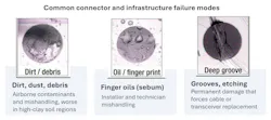
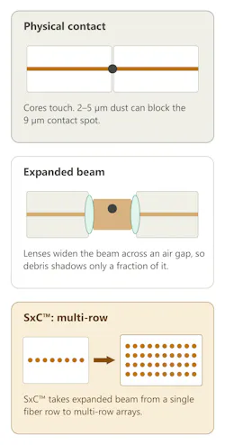
That monolithic part carries an expanded beam, and an expanded beam tolerates dust. A particle that would take down a butt-coupled link blocks only a fraction of a beam several times wider.
Nothing touches in the optical path, so debris can't scratch the surface. The same glass-and-air path handles enough power to carry an external laser source through the connector that carries the data.
Metrology is what makes four processes one process
Sequencing four fabrication methods creates four opportunities for errors to stack.
Metrology prevents that, which is why we list it as a fourth discipline rather than a quality step.
Every wafer that comes out of lithography is measured before the laser writes a feature, and the laser tool path is corrected to the datums measured on that specific wafer. Acceptance is based on optical performance, not a mechanical proxy. Because the substrate is transparent, internal features can be verified non-destructively after the part is complete.
The flow is designed to measure every unit. The part-to-part distribution of a lot comes from the parts themselves. The survey calls that distribution is the hardest thing to hold at volume. What holds it is measurement discipline, whichever process shaped the part.
Density at every edge: chip, package, box, rack and cluster
Shoreline density. The process that defines the lens sets lens pitch and fill factor, not mold-release angles or resist reflow. And because the fibers sit in a two-dimensional array instead of a single row along a V-groove, the chip edge gets more fibers per millimeter of shoreline.
Power. Glass end to end. As architectures move toward external and remote laser sources, the connector should not be the component that limits how much optical power the system can carry.
One technology, everywhere in the network. The same ferrule mates at the faceplate, backplane, optical engine, and laser source. That means a single qualification, a single spares strategy, and a serviceability model the field already understands.
Volume. Wafer-scale steps do the replication. The serial steps are confined to what only they can do. That is how a connector process scales to AI buildout volumes without linear growth in laser tools or in the risk each one carries.
Copper where you can, optics where you must, and a corollary
Astera's organizing principle for the copper-to-optical transition is good, and it deserves an extension for the connector itself: batch processes where you can, serial processes where you must, glass throughout, and metrology on everything.
The fiber-to-chip connector is becoming the component that decides how much of CPO's radix and power advantage reaches the system. No single fabrication method can cut the 3D geometry, place the lenses, build the mechanics, and measure the result. That takes four disciplines on one substrate.
About the Author
 Vivek Raghuraman
Vivek Raghuraman is the co-founder and CEO of Mixx Technologies. With over 20 years in the semiconductor industry, he’s launched groundbreaking products, including Broadcom's first co-packaged optics and Intel's silicon photonics transceiver. Holding seven patents, Vivek is an internationally recognized expert in silicon photonics and advanced packaging, advising the U.S. Department of Energy’s ARPA-E program, IEEE steering committee for photonics, the India Semiconductor Mission, and the Semiconductor Research Council’s MAPT program, shaping the future of semiconductor technologies. His cross-ecosystem leadership bridges national policy, deep-tech commercialization, and foundational R&D, accelerating the industry’s optical transition. At Mixx, his mission is to build scalable, reliable, and manufacturable optical infrastructure that forms the backbone of the next era of AI.